Introduction to 2 Layer PCBs
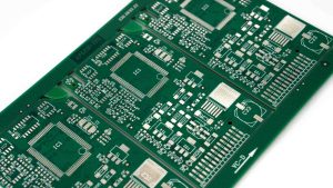
LHD TECH specializes in 2-layer PCBs, also known as double-sided PCB or two-layer PCB, which feature conductive copper on both the top and bottom layers. This printed circuit board design supports more advanced circuitry than single-layer boards while remaining cost-effective. Widely used in consumer electronics, industrial equipment, automotive systems, and medical devices, LHD TECH’s 2-layer PCB boards continue to meet the growing demand for compact, reliable, and affordable solutions in modern electronic components.
What Is a 2 Layer PCB Board?

A 2 layer PCB board (or 2-layer printed circuit) is a printed circuit board with two conductive copper layers positioned on the top and bottom layers of an epoxy or composite substrate. These layers are separated by a dielectric pcb base material, often FR-4, which provides the necessary mechanical support and insulation. The copper layer is etched to form electrical signal paths—circuit traces—that allow for dense, flexible circuit design on both sides of the board.
2 Layer PCB Basics
- Top and Bottom Layers of Conductive Copper:Offers more routing and component placement flexibility than a basic PCB with only one layer of copper.
- Vias (Small Holes on the PCB Board):Metalized (PTH – Plated Through Hole) to enable signals and power connections between the two sides of the board.
- Solder Mask and Protective Layer:Both sides are coated with a solder mask to prevent short circuits, protect the copper from oxidation, and define assembly areas.
- Silkscreen:Used on the pcb surface for labeling component placements and aiding in circuit board assembly.
2 Layer PCB Structure vs. Single Layer
| Feature | Single Sided PCB | 2 Layer (Double-sided) PCB |
| Copper Layers | 1 | 2 (top and bottom layers) |
| Signal Routing | One layer only | Both layers, interconnected via vias |
| Circuit Density | Low | Medium/High |
| Component Placement | One side | Both sides of the board |
| Cost | Lowest | Moderate |
| Complexity Supported | Simple/Basic PCB | Moderate/Advanced designs |
PCB Structure and Material Analysis
For double-layer PCBS, understanding the pcb structure and materials is the key to achieving the best performance and manufacturability.
To put it more straightforwardly: What materials are chosen and how the layers are stacked directly determine whether the board will be easy to use and manufacture in the end.
Key Layers and Materials
- Substrate Material:In the vast majority of cases, we use FR-4 fiberglass board, which strikes a good balance in terms of cost, durability and electrical performance, and can meet most regular requirements. Of course, if you have special needs, such as making high-frequency circuits or high-power equipment, we also offer PTFE, Rogers high-frequency plates or aluminum substrates to meet your requirements.
- Copper Layers:Both sides of the board are covered with standard 1-ounce (about 35 microns) thin copper layer. This thickness is sufficient for regular circuits. If the current in the circuit you design is particularly large, we also support thickening the copper to ensure the overcurrent capacity. The circuit graphics are precisely etched through the optical imaging process.
- Drilled Holes (Vias):The key to two-layer PCB plates lies in the connection. We use the through-hole plating technology to coat copper on the hole walls of the boreholes, allowing the current to freely shuttle between the top and bottom layers. This is a crucial step in achieving complex wiring.
- Solder Mask:of solder mask ink, which is the green oil that everyone sees (of course, there are also other colors). It mainly serves as an insulator to prevent accidental connection of solder joints and short circuits, while precisely exposing the pcb and pcba areas that need to be welded.
- Silkscreen:The white silk-screen layer on the board is printed with the bit numbers of the components (such as R1, C2), numerical values and our Logo. These small marks can help assembly workers identify at a glance where to place the parts, greatly reducing the risk of incorrect installation.
Common Substrate Materials
| Substrate Material | Dielectric Constant | Common Use Cases | Special Properties |
| FR-4 | 4.2–4.8 | Consumer/Industrial | Broad availability, good PCB for general use |
| PTFE | 2.0–2.6 | RF/High-frequency | Low loss, high-frequency applications |
| Rogers | 3.2–3.5 | Microwave/Military | Consistent performance at high freq. |
| Aluminum | N/A | Power/LED lighting | Superior heat dissipation |
How Do 2 Layer PCBs Work?
Unlike a basic PCB where all routing must occur on a single copper layer, a 2-layer PCB is built to leverage both the top and bottom layers for much more complex and dense circuit designs.
How Signals Flow
- Top Layer and Bottom Layer:Take the board of LHD TECH for example. Its top layer and bottom layer are not merely in a one-to-one relationship, but more like a three-dimensional circuit expressway network. Electrical signals can freely switch, cross and circle between the two layers of copper foil through the “vertical channel” of The power lines that supply power to the chips and the signal lines for data transmission are much more flexible when running.
- Vias (PTH):In simple terms, a via is a small hole drilled hole on a board. But the crucial step is yet to come: through the chemical copper plating process, a layer of copper is plated onto the small hole on the PCB, turning it into a through-hole. This tiny “elevator” connects the originally isolated top and bottom copper foils, allowing electrons to travel up and down on it, achieving a reliable electrical connection.
2 Layer PCB Manufacturing Process

From the perspective of our production process, making a double-layer PCB is actually adding several key steps specifically for double-sided boards on the basis of the traditional PCB technology.
The core lies in three things: make the first via and make it conduct; Second, evenly apply ink to both sides of the board. Third, ensure that the upper and lower layer lines can be stably connected to achieve reliable interconnection. Only by following these steps can we ensure that the board is not only usable but also practical and durable.
Step-by-Step 2 Layer PCB Manufacturing
- Material Cutting:First, cut the board size like FR-4 according to the dimensions provided by the customer. This step may seem simple, but only when the edge of the board is flat and the dimensions are precise can the subsequent processes be carried out smoothly.
- Drilling:Then comes the drilling. To drill through-holes and component holes on the PCB board, the position and precision of these small holes directly determine the reliability of the subsequent through-holes. This is the foundation.
- Electroless Copper Plating:After drilling, it enters the chemical copper deposition stage, where a thin layer of conductive copper is uniformly deposited on the hole wall through chemical reactions. A “bridge” was built for each small hole, electrically connecting the top and bottom copper foils.
- Pattern Imaging and Etching: How can I get the designed circuit diagram onto the board? First, apply a layer of photosensitive film. Then, shine ultraviolet light on the design draft. The areas that should be left are protected, while the areas that should not be left are exposed. Then, after etching, the unprotected copper is eaten up, leaving the required circuit patterns for the top and bottom layers.
- Pattern Plating and Tin Plating: After the circuit is etched, to prevent it from being damaged in subsequent processes, sometimes a tin protective layer is added to the circuit. This is actually a part of the electroplating process, especially when it is necessary to thicken the copper to enhance the current-carrying capacity or improve the transmission of high-frequency signals. This step can ensure that the circuit is both thick and safe.
- Solder Mask Application: After the circuit is completed, a layer of solder mask ink should be applied to both sides of the board (the most common color is green, but there are also red, blue and black ones). It is like a protective film, which serves two purposes: one is to prevent copper from being oxidized, and the other is to prevent accidental tin connection and short circuit during soldering. Where welding is needed, just “open a window” on the ink to expose it.
- Silkscreen (Legend Printing): The digit numbers (such as R1, C2, etc.), symbols and logos on the board are printed with epoxy ink. This layer is mainly for convenience. Whether it’s hand soldering or machine surface mount technology, you can tell at a glance which parts to place and it’s less likely to make mistakes.
- Surface Finish: Finally, the solder pads to be exposed for welding need to undergo surface treatment to ensure good welding and resistance to welding. Commonly used ones include lead-free tin spraying, gold plating, gold plating or OSP film. Tin spraying is inexpensive, while gold plating is suitable for fine circuits. Each has its own uses.
- CNC Routing and V-cut: The entire board has been pieced together for production and needs to be cut into the final size required by the customer with a CNC milling machine. If there are several units on a small board, V-cuts (V-shaped grooves) will also be added to facilitate the separation by hand in the later stage.
- Electrical Testing and Inspection: After the board is made, it must be checked through electrical testing to see if the circuits are unobstructed and if there are any short circuits. Flying probe testing is used for flexible spot checks, and then automatic optical inspection (AOI) is used to have the machine keep an eye on it to see if any circuits are damaged.
- Final Inspection and Packaging: In the final step, quality control personnel will conduct another appearance spot check in accordance with the IPC standards (usually the second or third level standards of IPC-A-600). After confirming there are no issues, clean thoroughly and vacuum pack for shipment. This way, it not only prevents moisture and oxidation but also makes it convenient for customers to assemble directly on the machine.
Cost Factors of 2 Layer PCBs
The cost of a 2 layer PCB—compared to other types of PCB—depends on a combination of material selection, board size, copper thickness, via count, finish, production volume, and lead time.
Major Cost Influencers
- Substrate Material:The conventional FR-4 offers the best value for money. However, if high-frequency circuits are to be made and special materials like PTFE or Rogers are used instead, the material costs will naturally increase.
- Copper Thickness:The standard is 1 ounce. If the current in the circuit is large, 2 ounces or even thicker copper foil is needed. The thicker the copper used, the higher the cost will naturally be.
- Board Size and Complexity:The larger the board, the denser the wiring, the more vias there are, or the line width and spacing are made particularly fine, the processing difficulty and working hours will increase, and the price will also be correspondingly higher.
- Surface Finish:The most economical one is OSP, and the most versatile one is lead-free tin spraying. If the board is fine, requires better reliability or is suitable for precise assembly, then ENIG gold is a good choice. Although it is a bit more expensive, it is indeed more reliable.
- Panelization:When designing, make good use of the spliced boards. Arrange several pieces on a large board to avoid material waste. When averaged out, the cost of each board can be saved a little.
- Production Quantity:For sample production or small batches, the engineering cost per piece is high, so it is naturally expensive. Once mass-produced, the cost per piece will drop significantly.
2-Layer PCB vs. Other Types of PCBs
We have always advised our customers: Choose the right board and you will achieve twice the result with half the effort. The key lies in taking out your specific application scenarios (such as consumer electronics, industrial control or high-frequency communication) and comparing them with other board types (like single-layer boards, four-layer boards, high-frequency boards) – from performance, cost to manufacturability, to see which one has the highest matching degree.
Single Sided PCB
like as one layer of copper,it just a simple structure and a low cost. It is suitable for jobs that do not have high requirements for circuits, such as simple LED light strips, electronic toys, calculators and so on. The drawback is that the wiring space is limited. When there are too many and too dense components on the board, it won’t function properly.
2 Layer PCB (Double Sided PCB)
This is what LHD TECH is best at and it is also the most mainstream in the current market. Both the top and bottom layers can be traveled conductive copper layer, making the design much more flexible. It can be used for circuits of medium complexity and has a high degree of integration. From mobile phones, smart home devices (that is, IoT devices) to automotive electronics and industrial control boards, its presence can be found everywhere. It’s sufficient and not expensive.
Multilayer PCB
When the performance of the board fails to meet the performance requirements of the product. Multilayer boards are made by pressing copper foil and insulating layers together like multi-layer cakes, with as few as 4 or 6 layers and as many as dozens of layers. It is specifically designed to serve those extremely complex large devices, such as servers, high-end laptops, smart phones, and communication base stations. It has strong performance and can run at high frequencies, but the corresponding design difficulty and manufacturing cost are also much higher.
Comparison
| Type of PCB | Layers | Application Complexity | Cost | Assembly Complexity |
| Single-Sided | 1 | Low | Lowest | Simple |
| 2-Layer (Double Sided) | 2 | Medium | Moderate | Moderate |
| Multilayer | 4–32+ | High | High | Complex |
Advantages and Limitations of 2 Layer PCBs
Key Advantages
- Increased circuit density:More components, less board size.
- Improved signal routing:Cross over traces with ease while maintaining signal integrity.
- Cost-effective for moderate complexity:With less money, circuits of medium complexity are manufactured, and the cost performance is also achieved to the extreme
- Widely used and supported:Nowadays, every PCB factory in the market has a mature production line. Even if you want to make a sample quickly, it is not difficult to achieve.
- Better electromagnetic compatibility (EMC):Because there are two layers of copper, you can skillfully use one layer for power supply and the other for flooring. The detailed division of labor provides a shielding cover for the signal, enhancing the noise resistance and electromagnetic compatibility, and making the board run more stably.
Limitations
- Power distribution:Not as strong as multilayer PCBs with dedicated inner layers for plane distribution.
- High-frequency limitations:Top and bottom layers can only do so much—high-speed, high-frequency signals may require additional ground reference or inner layer.
- Extremely dense BGAs:Might be better handled with more pcb layers and advanced via techniques.
Applications of 2 Layer PCBs in Modern Electronics
2 layer printed circuit boards are at the heart of modern electronic devices.
Widely Used Application Areas
- Consumer Electronics:
- Smartwatches, thermostats, remote control units, IoT modules, electronic toys.
- Automotive:
- Control panels, entertainment modules, basic sensors, LED driver circuit boards.
- Industrial Automation:
- PLC interfaces, industrial sensor nodes, relay control boards.
- Medical Devices:
- Patient diagnostic equipment, wearables, portable test instruments.
- Telecommunications:
- Ethernet interfaces, routers, basic USB and RS485 converters.
- LED Lighting:
- LED drivers, arrays, and converters for home and commercial illuminations.
- Power Systems:
- Power management modules, DC-DC converters, small inverters.
2-Layer PCB Design: From Beginner to Expert

Beginner’s Essentials
- CAD Tool Selection:Find a handy CAD software that supports double-layer board layout, such as KiCad, Altium, or Eagle. Convenience can save you a lot of effort.
- Component Library Management:Make sure in advance that the packaging used is consistent with the actual product so as not to make mistakes during assembly later.
- Modular Design Blocks:First, cut the circuit into blocks by function, such as separating the power supply, main control, and analog/digital sections.
- Board Edge and Connector Placement:During the planning stage, the connectors and installation positions are set at the edges of the board to achieve the purpose of convenience and stability.
Advanced 2-Layer PCB Design Tips
- Signal Integrity Focus:High-frequency signals should be routed as short as possible with fewer turns. At the same time, more ground copper should be laid in blank areas to provide a clean reference plane for the signals, which can effectively reduce interference.
- Via Optimization:The vias should be distributed reasonably, and more should be added at key positions (such as under the high-current path). If used properly, it can not only reduce impedance but also help dissipate heat.
- Power/Ground Strategy:For high-current circuits, the traces should be wide and more vias should be drilled. Especially under the voltage regulator or near the BGA pad, doing so can prevent insufficient power supply or overheating.
- Top and Bottom Layer Usage:It is usually recommended that signals be routed on the top floor and power and ground be laid on the bottom floor. But this is just a conventional approach. How to make the specific classification still depends on your actual circuit requirements and can be flexibly adjusted.
Choosing the Right 2 Layer PCB Manufacturer
In LHD TECH’s view, choosing the right PCB partner makes a real difference whether your double-layer board is just passable or both stable and reliable.
Let’s have a brief chat about what a good partner should have
- Certification:It is essential to choose a company that has solid certifications such as IPC, ISO, and UL.
- Technology Capabilities: We can consider them from aspects such as fine pitch, small aperture, gold plating (ENIG) process, or impedance control.
- DFM Support: Proactively conduct manufacturability analysis (DFM) before production starts? Can minor flaws in the design be detected in advance? This step saves time and cost.
- Testing and Inspection: Is flying probe testing, open and short circuit testing, and automatic optical inspection (AOI) standard before shipment? Only products that are dispatched with test reports can be regarded as qualified.
- Transparent Quoting and Communication: materials, surface treatment, engineering cost, testing cost… Please list each expense and cost clearly. If there is a version change or DFM feedback during the process, we can respond quickly in the first place.
- Prototype and Production Expertise: Fast prototyping in the early stage and stable large-scale production in the later stage. A manufacturer that can cover the entire product life cycle can accurately understand customer needs.
Soldering and Assembly Tips for Double-Sided PCBs
In the LHD TECH team, we are well aware that assembly is the final step that determines the reliability and performance of double-layer boards. Since the components may be distributed at the top and bottom layers, every step of assembly must be handled with great care.
Reflow and Wave Soldering
Reflow Soldering for SMT: How to solder when there are surface mount parts on both sides? Generally, the side with more or heavier components is welded first. After welding and cooling, turn it over and weld the other side. The key is to control the temperature well so as not to melt the already welded part on the other side.
Wave Soldering for Through-Hole: If there are plug-ins (PTH) on the board, wave soldering comes in handy. If there are surface mount parts on the bottom, they need to be glued together before passing through the wave peak; otherwise, they will be washed away by the solder.
Selective Soldering: Nowadays, many boards are mixed with patches and plugins. By using selective soldering, you can spray solder only onto the pins of the plug-in components without damaging the adjacent surface mount parts.
Assembly Best Practices
Stencil Thickness: When the components on the board are of different sizes, the thickness of the solder paste must be accurately controlled. If it’s too thick, it’s prone to solder bonding; if it’s too thin, there’s a fear of false soldering. A balance point needs to be found.
Component Placement Sequence:
Thermal Relief and Vias: Provide sufficient thermal relief for ground pads and use thermal vias for components dissipating power, distributing heat between top and bottom layers.
Assembly Quality Tips
- Avoid Tombstoning:Small patch parts are prone to lifting at one end. The key is to measure the solder paste evenly, have the reflux curve correct, and ensure that both sides melt and are subjected to force simultaneously, avoiding one side being hot and the other cold.
- Manual Touch-Up:When making a sample, it is inevitable to make a few manual additions. The temperature of the soldering iron should be well controlled, especially beside the vias or on small pads. If it is heated for too long, the pads are prone to fall off.
- Inspection:Those with dense boards and BGA are not visible to the naked eye. We need to go through the AOI scan and then use an X-ray to check if there is any solder connection or false soldering at the bottom solder joints.
Quality Issues in 2 Layer PCB Production
No matter how good the initial design, careful attention is needed during PCB manufacturing and assembly to minimize defects in 2-layer PCBs.
Common Quality Challenges
- Open/Short Circuits:Can result from incomplete etching, poor solder mask alignment, or solder bridges during assembly.
- Insufficient Via Plating:Inadequate copper in vias (from poor plating or contamination) leads to unreliable connections between layers.
- Silkscreen Misalignment:Misplaced reference designators or polarity marks can result in assembly errors.
- Warping/Delamination:Excessive PCB base heating or poor lamination technique causes mechanical instability, impacting fit or performance in enclosures.
- Surface Finish Defects:Incomplete surface finish can cause solderability problems or rapid aging of exposed copper.
Strategies for High-Quality PCBs
- Choose the Right Manufacturer:Only work with PCB manufacturers offering Class 2 or 3 quality, especially for critical boards.
- DFM Reviews:Take advantage of DFM (Design for Manufacturing) checks—most modern PCB manufacturers offer these as part of their service.
- Inspection and Testing:Specify full electrical and functional tests for production. For high-reliability, request cross-section analysis and advanced AOI.
FAQs on 2 Layer PCBs
Q: Can I use a 2-layer PCB for high-frequency applications?
A: Yes, if you follow sound layout practices—short, matched traces, continuous ground pours, and high-quality substrate material (like PTFE or Rogers)—a two-layer PCB can support moderate high-frequency circuits up to several hundred MHz. For ultra high-frequency or microwave, multilayer PCB manufacturing is usually better.
Q: How do I select copper thickness for my double-sided PCB?
A: Standard is 1 oz/ft² (≈35µm); increase to 2 oz/ft² (≈70µm) for higher current paths, such as power supply circuits, but this may affect trace width and spacing minimums—always consult your manufacturer’s capability tables.
Q: How do I manage test and debugging on double-sided PCBs?
A: Include labeled test points/pads accessible from both top and bottom, and keep traces near these points short to ensure signal fidelity. For complex or densely packed boards, a test header is invaluable.
Q: Can I mix SMT and through-hole components on a two-layer PCB?
A: Absolutely—modern PCBs are usually designed with both. Just coordinate your assembly sequence (SMT reflow, then through-hole wave or hand soldering).
Q: Why are double-sided PCBs so widely used in consumer electronics?
A: They strike a perfect balance: supporting moderate circuit complexity and compact board size, yet are cost-effective and much simpler to manufacture than multilayer boards.
Future of 2 Layer PCBs
As electronic devices evolve, 2 layer PCBs remain a mainstay of design and manufacturing:
- Continued Relevance: The double-sided PCB is expected to dominate mid-level complexity products—IoT modules, wearables, industrial control—well into the future, thanks to robust manufacturing ecosystems and excellent price/performance.
- Innovation in Materials: Adoption of higher grade, eco-friendly substrates and increasingly fine feature sizes are making two-layer PCBs even more versatile.
- Hybrid Approaches: Some designers combine a compact multilayer PCB for dense, high-speed cores with a two-layer PCB for interface or power modules—balancing performance, cost, and ease of modification.
- Advanced Prototyping: With fast, affordable PCB prototyping now globally available, engineers rapidly iterate on two-layer PCB designs, getting products to market more quickly and with fewer design flaws.
Conclusion
The 2 layer PCB—or double-sided PCB—remains a pillar of modern electronics. Its unique construction, with a copper layer on both sides of an insulated substrate, brings unparalleled flexibility to designers striving for performance, fast time-to-market, and cost-effectiveness. As printed circuit boards for new devices get smaller and smarter, double-sided boards continue to balance signal integrity, circuit density, and manufacturability for a vast range of applications in consumer electronics, industrial automation, automotive, medical, and more.