Introduction
At LHD TECH, we’re in the heart of today’s electronics manufacturing—a fast-moving world where the challenge never stops. We are continuously committed to achieving a dynamic balance among our three core goals: ensuring zero defects in product functionality, minimizing process defect rates, and simultaneously enhancing production throughput efficiency and cost-effectiveness throughout the entire process. The relentless pursuit of quality control, yield optimization and capacity enhancement has been internalized as the core operational paradigm of our advanced manufacturing system. Through real-time monitoring and closed-loop management on the digital production platform, precise collaboration is achieved in daily production.
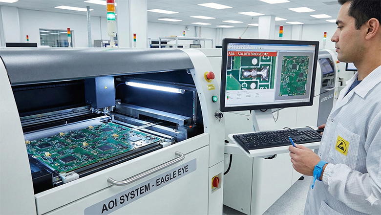
That’s where Automated Optical Inspection – or AOI – comes in. Think of it like a super-smart, high-speed quality inspector for circuit boards. It uses machine vision really sharp cameras and clever software to scan every little part on a PCB automatically, catching flaws that humans could easily miss.
Honestly, trying to inspect these modern, super-detailed boards by hand just doesn’t cut it anymore – it’s too slow, too tiring, and too unreliable. So now, pretty much everyone in the industry uses AOI. It’s become a must-have tool if you want to meet today’s tough quality standards.
What does AOI quality control requirements actually do for you? It checks everything thoroughly, keeps the production line moving fast, and finds all kinds of defects – from misplaced parts to bad solder connections – that could cause a finished product to fail later on.
In this article, we’re going to break it all down: how role of AOI really works, the different types of systems out there, what kinds of problems they catch, how to actually set one up, how they compare to other inspection methods, and what cool new developments we can expect in the future.
What is Automated Optical Inspection (AOI)?

So what is Automated optical inspection (AOI) , exactly?
Think of it as a high-resolution imaging and advanced optical systems for checking printed circuit boards. It’s a specialized way to spot problems — usually right after tiny parts are placed on the board during the SMT stage.
In today’s factories, AOI isn’t just a nice-to-have — it’s a core part of making sure products are built right. This system scans the whole board with super-clear cameras and smart optics, looking at everything that matters:
- Are all the parts actually there?
- Are they in the correct position?
- Are the solder joints good and solid?
- Even small stuff — like too much solder paste or bits of dust or debris — doesn’t escape its notice.
Basically, AOI catches the kinds of flaws that could cause a device to fail later on — all automatically, without slowing things down.
AOI Systems: Inspection Technology Essentials
Based on the summary of our manufacturing experience ,we believe the core of any AOI system is its optical and image processing capability.
AOI systems use a combination of:
- High-Resolution Cameras:To capture detailed images of the entire PCB or specific zones.
- Sophisticated Lighting Systems:Ensuring that all parts, including hidden or shadowed areas, are illuminated appropriately.
- Image Processing Software:For comparing the captured images against digital reference data (such as Gerber files or CAD models), and identifying discrepancies or defects.
Our automated optical inspection system has achieved high-precision full-process inspection coverage for printed circuit boards. Through this technology, each circuit board is strictly verified in accordance with the original design parameters to ensure that its electrical performance is completely consistent with the design specifications, achieving zero functional deviation. At present, this technology has become an indispensable core link in quality control for all the industries we serve.
For this reason, AOI is a comprehensive inspection tool in manufacturers ranging from cutting-edge consumer electronics to high-reliability automotive electronics and aerospace control systems all trust LHD TECH to provide them with product solutions that meet strict quality and reliability requirements. Whether in high-volume production environments, multi-variety flexible production lines, or in critical application fields with zero-defect requirements, automated optical inspection systems are always comprehensive and precise inspection guarantees for ensuring product quality.
Why Automated Optical Inspection is Critical in Modern PCB Manufacturing

Honestly, in today’s electronics manufacturing world, you can’t really do without automated optical inspection systems anymore. Here’s why they’re absolutely essential in every modern circuit board production line:
Benefits of AOI in Manufacturing Process
- Increased Inspection Accuracy:AOI systems provide reliable, repeatable inspections at speeds and scales that manual inspection cannot match, even in high-speed production lines.
- Enhanced Defect Detection:AOI allows operators to detect a variety of defects in real-time, including solder bridges, component misalignment, missing or wrong components, and insufficient/excess solder.
- Quality Control and Traceability:AOI generates digital inspection records for every board, supporting stringent traceability and quality management system audits.
- Automated Inspection for Maximum Throughput:AOI systems can inspect hundreds or thousands of boards per hour, keeping pace with the fastest SMT lines.
- Reduced Labor Costs:The shift from manual inspection to automated inspection systems improves efficiency, minimizes fatigue-related errors, and frees up skilled personnel for higher-value tasks.
AOI gets used so much because it’s like a double win for factories. First, it catches bad boards before they move down the line—so fewer duds slip through. But maybe just as important, it’s not just about saying “this one’s bad.” It actually helps the whole process get better.
The AOI system collects real data that tells the engineers exactly what’s going wrong. With that info, they can fine-tune things like:
- The heat settings in the reflow oven.
- How accurately the machines place parts.
- How often they clean the stencils that apply solder paste.
How Does Automated Optical Inspection Work?
The AOI system integrates high-precision machine vision hardware and intelligent image processing algorithms to achieve high-speed and highly repeatable automated inspection tasks. Its workflow can be decomposed into the following core stages:
- Image Capture:The AOI system moves either the PCB or cameras to cover all areas of the board. Multiple high-resolution cameras capture top-down and sometimes angled images.
- Lighting and Illumination:AOI systems use specialized lighting—RGB, white, or UV—to ensure even illumination and highlight specific features for detection accuracy.
- Image Processing:The captured image is compared to a reference “golden board” or directly with design data (such as CAD/Gerber files) using various algorithms.
- Defect Identification and Classification:The AOI system uses template matching, feature recognition, and statistical pattern matching to detect deviations from the design. Defects are automatically classified—critical, major, or minor.
- Inspection Reports and Data Integration:Inspection results are digitized for each board, supporting production traceability, trend analysis, and process control.
AOI Inspection Tasks Across Manufacturing Stages
| Inspection Task | AOI Application | Benefits in PCB Production |
| Bare Board Inspection | Pre-SMT, post-fabrication | Detects etch errors, open circuits, via defects |
| Solder Paste Inspection | Pre-component placement (SPI) | Quality assurance of solder paste volume, minimizes tombstones |
| Pre-Reflow Assembly Inspection | After component placement | Catches missing, misaligned, or skewed components early |
| Post-Reflow AOI | After SMT soldering | Detects solder bridges, open solder joints, lifted leads |
| Final Assembly Inspection | Post-assembly/pre-packaging | Ensures finished board integrity, correct labels, cleanliness |
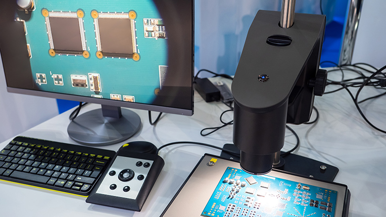
Detection Principles and Inspection Mechanisms in AOI
We believe that the core advantage of AOI technology lies in its deep integration of advanced machine vision and precise optical system design, and through powerful image analysis algorithms, it can accurately capture and determine micron-level defects. Based on this technical concept, the detection system of LHDT TECH mainly adopts the following mainstream detection mechanisms:
- Template Matching:The system overlays board images with a reference template, flagging any deviation.
- Pattern Matching & Statistical Pattern Matching:AOI systems learn the expected geometric or statistical properties of features, so even subtle deviations from normal patterns are flagged.
- Object Recognition & Blob Analysis:Used to detect abnormal sizes, missing features, solder balls, or misplaced parts.
- Feature-Based Algorithms:AOI technology isolates and analyzes features like solder joint fillet shape, lead coplanarity, or pad position.
- Machine Learning / AI Algorithms:Advanced AOI systems now include neural networks trained on millions of defect samples, allowing them to adapt to new defect types.
2D AOI systems inspect traditional surface-level features, while 3D AOI systems add volumetric data—enabling precise measurement of joint coplanarity, paste height, and more. Advanced 3D AOI systems can even identify defects in hidden joints that 2D inspection cannot.
Defects Detected by AOI Systems

One of the core advantages of AOI technology lies in its broad-spectrum defect detection capability that surpasses the limits of human labor. The detection system of LHDT TECH can accurately identify and automatically classify defects including but not limited to the following categories:
In PCB Assembly:
- Solder Bridges and Shorts:Unintended connections between leads and pads, which can cause electrical shorts and catastrophic failures in the field.
- Component Misalignment or Skew:Misplaced or skewed components compromise PCB functionality, especially in high-speed digital or RF circuits.
- Lifted Leads:Leads not properly bonded to solder pads, often causing intermittent defects.
- Wrong or Missing Components:AOI systems can inspect the board using design data to detect incorrect parts or component value mismatches.
- Insufficient or Excess Solder:Both conditions can lead to unreliable joints; advanced 3D AOI systems offer precision measurement of solder volume and shape.
- Tombstoning:A one-sided elevation of chip resistors or capacitors, typically caused by uneven heating or solder volume.
- Cold or Cracked Joints:AOI with high-resolution imaging can spot incomplete wetting or micro-cracks in solder.
- Solder Balls and Debris:Foreign material that may cause short circuits or inhibit proper reflow.
In Bare Board and PCB Fabrication:
- Open Circuits and Trace Interruptions:Issues in copper etching that prevent proper connectivity.
- Copper Residues and Slivers:Remaining conductive debris from improper etching, increasing the risk of shorts.
- Line Width Violations:Tracks or pads that deviate from manufacturing specifications due to process drift.
- Via Defects:Undersized, blocked, or incompletely plated vias that disrupt signal continuity.
AOI systems are seriously fast and consistent. AOI systems can inspect hundreds of PCBs per hour, and they do it with extreme accuracy. This holds true even as components get tinier and boards get more crowded than ever.
Types of AOI: 2D AOI Systems and 3D AOI Systems
We are well aware that there are essential differences in the technical solution types of AOI systems. Therefore, one of our core services is to provide professional technical assessment for clients and assist them in understanding the characteristics and applicable scope of various detection technologies. Choosing the optimal detection system is not a standardized decision, but entirely depends on the specific process characteristics of your production line, the complexity of your products, and the established quality control indicators. We will collaborate with you to conduct a technical adaptation analysis and provide you with a customized AOI solution configuration plan based on your specific process and inspection requirements.
2D AOI Systems
- How They Work:2D automated optical inspection systems use top-down imaging to analyze surfaces. They excel at checking for component presence, simple soldering defects, and misplacements where height is not a concern.
- What They Inspect Best:Surface features—missing chips, misplaced parts, insufficient solder, visible bridges, and polarity.
- Typical Applications:Inline inspection for mid-density PCB, pre-reflow and post-reflow AOI, and bare-board visual inspection.
3D AOI Systems
- How They Work:3D AOI systems expand on 2D capabilities by using structured light or laser triangulation to capture height and volume data for every inspected feature.
- What They Inspect Best:Solder joint volume, coplanarity issues (BGA balls, QFNs), height measurement, and defects hidden from 2D cameras.
- Typical Applications:Critical post-reflow inspection, boards with BGAs, high-reliability industrial and automotive electronics.
| Feature | 2D AOI Systems | 3D AOI Systems |
| Inspection Coverage | Surface-level, visible defects | Volume, coplanarity, hidden joints |
| Inspection Parameters | X/Y position, area, color | X/Y/Z position, area, height, volume |
| Speed | Fast, suitable for most lines | Slightly slower, more data-rich |
| Use Case | Inline, general SMT, bare boards | Advanced, BGA/QFN, automotive/medical |
Advantages and Limitations of AOI Technology
Advantages
- Consistent and Repeatable Inspection:AOI removes the human factor, ensuring each board is inspected to identical criteria.
- Precision and Speed:AOI can inspect at line speeds far beyond human capability, and with true micron-level accuracy.
- Comprehensive Inspection:AOI systems inspect the entire population of boards, not just samples, so escaped defects are nearly eliminated.
- Traceability and Data Analytics:Each inspection is logged and can be traced back by serial, lot, zone, or even defect class, allowing robust quality control system performance analysis.
- Modular and Scalable:AOI allows staged implementation and can be upgraded from basic (2D) to advanced (3D) versions, supporting a growing range of inspection requirements as products change.
Limitations
- Inability to Inspect Internal/ Embedded Defects:While AOI excels at surface anomalies, it cannot “see” inside solder joints or beneath opaque components (for these, Automated X-ray Inspection is the answer).
- Setup and Maintenance Complexity:Initial programming and tuning of AOI parameters require time, deep knowledge of the manufacturing process, and operator skill.
- False Positives/Negatives:If inspection criteria are set too narrowly or too loosely, AOI might flag good boards as defective or miss borderline faults.
- Cost:The up-front investment is substantial, though it pays off quickly through yield improvement and cost reduction.
Automated Optical Inspection vs Manual Inspection and Other Methods
Comparing automated optical inspection systems with manual inspection methods and other automated inspection types helps clarify AOI’s role in modern manufacturing.
| Inspection Method | Pros | Cons | Suitability |
| AOI (2D/3D) | Fast, repeatable, high throughput | Surface-only, setup complexity | All SMT/PCBA lines |
| Automated X-ray (AXI) | Internal/hidden features | Slower, higher investment | High-reliability, BGA |
| Manual Inspection | Flexible, visual context | Slow, inconsistent, fatigue-prone | Very low-volume, protos |
| In-circuit Test | Functional, electrical test | Limited to non-visual, test access needed | Final test, functional boards |
| Laser Test/ALT | Dimension, coplanarity | Geometry only, not electrical | Tall/odd-shaped parts |
AOI helps bridge the gap between inline speed and quality assurance, providing the backbone for any robust quality control system. Manual inspection can never match AOI’s speed or defect detection rates in high-mix, high-density environments.
Best Practices and Implementation of AOI
Achieving maximum value from AOI depends on smart implementation of AOI technology and best practices, from initial setup through daily operation.
- Design for AOI:Ensure your PCB layouts allow clear visual inspection, adding fiducials and minimizing shadow zones.
- Stage AOI Across the Line:Use AOI early (pre-reflow, solder paste) and late (post-reflow, final inspection) to catch errors when they are cheapest to fix.
- Integrate AOI Data:Feed results into MES or ERP for trend analysis and yield management.
- Regular Calibration & Training:Schedule preventive maintenance, update libraries, and invest in operator and programmer development to ensure reliable results.
- Continuous Process Feedback:Use AOI analytics to find root causes (e.g., mounter drift, solder paste variations) and drive real improvements in the manufacturing process.
Future Trends in AOI Technology

The future of AOI technology is shaped by rapid advances in hardware, software, and Industry 4.0 integration:
- Artificial Intelligence and Deep Learning:AOI systems increasingly leverage AI to adapt to new defect types and automatically tune inspection parameters—even as board designs evolve.
- Edge Computing and Real-Time Analytics:Next-gen AOI systems analyze data locally, offering instant response to line issues and enabling predictive maintenance.
- Hybrid and Multimodal Inspection:AOI combined with X-ray, laser profiling, or infrared inspection ensures comprehensive defect coverage, even on the most advanced boards.
- Industry 4.0 Integration:AOI data is now fed directly into enterprise resource planning systems, enabling intelligent process optimization and supporting closed-loop feedback in smart factories.
- Advanced Imaging Technologies:Cameras with resolution enhancements, hyperspectral imaging, and improved optics continue to increase inspection accuracy while expanding the range of detectable faults.
Frequently Asked Questions About AOI
Q: What makes automated optical inspection systems different from traditional visual inspection?
A: With AOI, it’s all about the tech—sharp cameras, smart lighting, and clever software. It’s way more reliable than human eyes, checks every single board without slowing things down, and keeps perfect records of every flaw it finds. Basically, it’s faster, doesn’t get tired, and catches stuff people often miss.
Q: Are 2D AOI systems still widely used, or are 3D AOI systems required for modern manufacturing lines?
A: Both are still very much in play. 2D AOI systems are great for most standard checks—they’re affordable and get the job done well. But as boards get packed with more hidden parts like BGAs and tight components, 3D AOI systems becomes pretty essential. It measures height and volume in ways 2D just can’t, so you often need both depending on what you’re building.
Q: How does AOI integrate with other inspection or quality control systems?
A: AOI usually plays the lead role in quality control. It teams up with tools like X-ray inspection or in-circuit testers to cover all the bases. Plus, modern AOI can send its data straight into factory management software, so engineers can spot trends fast and fix issues before they pile up. It’s all about keeping the line smart, connected, and running smooth.
Q: What are common pitfalls in implementation of AOI?
A: Common challenges include poor initial programming, neglecting regular calibration, and ignoring AOI data rather than using it for process improvement. Success stems from clear inspection criteria, continual software and hardware updates, and cross-functional team involvement in AOI integration.
Q: What are future trends in AOI I should plan for?
A: Expect continued growth in machine vision, advanced 3D AOI, and AI-powered automated inspection. Multimodal and edge-based AOI technologies, combined with smart factory integration, represent the future of AOI, increasing inspection accuracy and minimizing escapes in extremely complex PCBs.
Conclusion
As LHDT TECH, we have deeply realized in practice that automated optical inspection (AOI) technology has reshaped the PCB quality inspection paradigm in the electronics manufacturing industry. From the evolution of basic visual tools to today’s intelligent inspection systems, its development process has confirmed the irreplaceable core value of this technology in ensuring quality, optimizing costs and driving the process of intelligent manufacturing.
Our AOI solution provides customers with
- Consistent, high-speed inspection
- Comprehensive inspection of every board, every time
- Automated detection and classification of defects—from misses to solder bridges to component misplacements
- Robust data for quality control, process improvement, and traceability
By deploying LHDT TECH’s modern AOI system, manufacturers can build the optimal inspection strategy, continuously improve the yield rate in the context of the rapid iteration of PCB technology, and achieve the goal of zero-defect delivery.
Takeaways and Recommendations:
- Design collaboration: Incorporate detectability design criteria during the PCB design stage, and configure 2D/3D fusion inspection solutions based on inspection requirements, deeply integrating AOI into the quality management system
- Closed-loop optimization: Establish a process feedback mechanism based on AOI data to achieve root cause analysis of defects and real-time process correction
- Forward-looking layout: Actively explore our next-generation intelligent inspection solutions that integrate AI algorithms and Industrial 4.0 interfaces
Final Thought: With the sharp increase in PCB complexity and the increasingly strict requirements of end customers, the adoption of advanced AOI technology has shifted from an option to a key element of core competitiveness. LHDT TECH Considers and implements AOI helps manufacturers rise above the challenges of modern inspection and establishes a new benchmark for quality, efficiency, and reliability.