Introduction: Through-Hole Technology’s Vital Role in Modern Electronics

In the rapidly evolving field of electronics and advanced PCB design, some technologies withstand the test of time while continuously meeting new industry demands. Through-hole technology is one such example.Through-Hole Technology forms a fundamental foundation in the manufacturing of printed circuit boards. This technology provides electronic systems with outstanding reliability, robust structural characteristics and excellent performance, thereby continually solidifying its central role in the industry.
Surface mount technology and high-density miniaturized components have achieved rapid development. In demanding application fields such as industrial automation, aerospace, medical devices and power equipment, the design and manufacturing of electronic devices still rely on through-hole technology to play its critical role. These fields place continuous demands on connection strength and electrical reliability, and it is precisely these demands that continually drive the evolution of through-hole technology in new directions.
Why Through-Hole Technology Endures
Through-hole assembly is renowned for:
- Its ability to handle high power and high-voltage circuits
- Electronic components must operate continuously over extended periods under mechanical stress and vibration environments. Their reliability must be fully ensured under such conditions.
- For products that need to operate stably for decades, long-term reliability is a core indicator that must be achieved during the design phase. In the design process of such products, durability and stability are consistently regarded as central considerations.
- This technology covers the complete and coherent full process from prototype design to verification testing, accommodates the production and operation demands of multi-category, differentiated and low-volume scale, and boasts practical application adaptability with an extremely wide coverage range.
Through-Hole Technology, based on its continuous technological iteration process and current industry development trends, remains an irreplaceable core solution in the field of electronics manufacturing. This technology seamlessly integrates market-proven mature traditional processes with breakthrough cutting-edge innovative technologies, and by virtue of highly compatible hybrid assembly models and green low-carbon sustainable production solutions, it continuously adapts to and meets the ever-upgrading diversified market demands of the electronics industry.
Understanding Through-Hole Technology in PCB Assembly
Types of Through-Hole Components
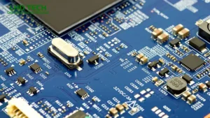
Through-Hole Technology employs the method of accurately inserting component leads of specific specifications into the plated holes of a printed circuit board, and achieves electrical connections with stability and durability through standardized soldering processes. Surface-Mount Technology directly and accurately mounts various micro-components onto the surface of the designated functional areas of the printed circuit board. Compared to this, through-hole assembly enables deeper-level mechanical fixation and electrical connectivity. This unique characteristic of forming deep connections gives it indispensable importance in the manufacturing of highly reliable electronic products.
| Component Type | Description | Example Use Case |
| Axial Lead | Leads out both ends; laid horizontally | Resistors, diodes |
| Radial Lead | Both leads exit same side, stand vertically | Electrolytic capacitors |
| DIP (Dual-Inline) | Two rows of parallel pins | Microcontrollers, ICs |
| SIP (Single-Inline) | One row of pins, saves space | Logic modules, resistor packs |
| Power Connectors | Multi-lead, handle higher currents | Mains, I/O, board interconnects |
How Through-Hole Assembly Works
Modern PCB assembly manufacturers combine manual assembly and advanced equipment in their practical production processes.
- Axial/radial insertion machines handle high-throughput, repetitive placements.
- Manual placement is used for complex boards, odd-form components or prototyping.
- Soldering techniques:Wave, selective and laser soldering ensure full penetration of solder, optimal joint formation and minimal defects.
- Automated optical inspection (AOI) is deployed for quality control, ensuring every lead is soldered correctly and all connections are secure.
When and Why Through-Hole is the Optimal Choice
In the following specific application requirements and specialized environments, through-hole assembly technology is typically adopted by manufacturers.
- Circuits must handle high power, current or voltage.
- When subjected to various complex and harsh operating conditions such as vibration, high temperature and mechanical shock, the relevant electronic components must always maintain extremely high functional reliability with stable operational performance. This stringent requirement is commonly found in special application fields such as aerospace and automotive electronics. These fields formulate and implement a series of stringent specifications and standards for the operational stability of circuits.
- The design of infrastructure and industrial electronic products should be flexible enough and also allow for maintenance operations at the application site.
- The cost and risk of failure outweigh any board real estate savings.
Key Benefits and Strengths
- Resilience and robustness:Ideal where robustness takes priority over miniaturization.
- Superior electrical and mechanical performance:Ensures long-term reliability in key circuits.
- Easy repair and upgrades:Components are easier to replace or upgrade in the field.
- Thermal performance:Handles thermal cycling, high-power dissipation and environmental extremes better than delicate SMT pads.
- Enabling new form factors:Miniaturized through-hole options blend reliability with shrinking circuit board designs.
Common Mistakes and Tips
- Don’t skimp on plating:High-quality, fully plated-through holes are essential for long-term solder and high-current reliability.
- Account for form factor changes:Tighter lead pitch improves density, but makes hand assembly more challenging.
- Isolate power and sensitive analog:
- Avoid routing high-speed signals beneath through-hole power connectors.
- Always optimize pad sizes for the latest miniaturized through-hole packages.
- Consult early with assembly partners:They’ll help select the ideal process for your board—avoiding costly rework or design changes.
Through-Hole Technology vs. SMT: Comparing Approaches in Modern PCB Design
PCB assembly processes continue to evolve. Discussions surrounding the applications of through-hole technology and surface mount technology (SMT) remain lively in the field of modern electronic manufacturing.
Technical Comparison
| Aspect | Through-Hole Technology | SMT (Surface Mount Technology) |
| Mounting | Lead inserted in plated holes, soldered below | Small pads directly on PCB surface |
| Component Size | Larger, robust | Miniaturized, for high-density layouts |
| Assembly Process | Manual or automated insert + solder | Automated pick-n-place + reflow solder |
| Mechanical Strength | High—resistant to mechanical stress and vibration | Moderate—sensitive to shock and flex |
| High Power Handling | Excellent (can handle higher current/voltage) | Good for low-moderate power levels |
| Repair/Rework | Easier hand replacement | More difficult, may need hot air tools |
| Density/Real Estate | Lower—takes up more board space | Superior, enables shrinking of form factors |
| Cost Efficiency | Costlier for high volume, but essential for reliability-critical builds | Most cost-effective for mass production of compact consumer devices |
Applications and Industry Insights
In the world of electronics manufacturing, the decision between SMT and through-hole is shaped by end-application demands.
- Automotive & Aerospace:Through-hole dominates for engine controls, main connectors, relays and modules subjected to temperature cycling or mechanical vibration.
- Telecommunications & 5G Rollout:High-frequency applications often leverage both—SMT for tiny RF transceivers and high-density circuits, through-hole for board-to-board connectors handling high-speed data.
- Industrial & Power Electronics:Circuit boards handling heavy loads, high power, or field-upgraded control systems benefit from the mechanical stability and current-handling ability unique to through-hole technology.
Future Trends in Through-Hole Technology: Key Trends and Emerging Solutions

Miniaturization: Meeting the Demands for Smaller, Smarter Circuits
One of the most noticeable future trends in through-hole technology is the industry’s adaptation to miniaturization. As the market for modern electronics expands into wearables, smart sensors and IoT. PCB assembly manufacturers now offer:
- Through-hole components with tighter lead pitch specifications can effectively achieve higher integration density per unit area of each printed circuit board.
- Micro-DIP, miniaturized electrolytic capacitors, and fine-pitch connectors designed for compact PCBs in medical, automotive and telecom devices.
High-Frequency Applications and the Rollout of 5G Networks
Emerging technologies such as 5G put forward higher requirements for electronic components. Electronic components must reduce the distortion phenomena of various signals during the transmission process to the minimum extent and support stable and reliable high-speed data transmission. The core development trends in the relevant fields specifically include:
- Through-hole connectors with gold, silver or OSP plating that maintain low resistance and signal integrity in RF and high-frequency PCB designs.
- Use of materials with low dielectric loss (PTFE, ceramics) in through-hole circuit sections, improving performance for radio-frequency PCB and microwave circuits.
Combining Through-Hole and SMT in Mixed-Technology Builds
Modern PCB assembly services increasingly integrate both approaches:
- Hybrid printed circuit boards use through-hole for high-current, high-reliability connections (power, relays, large connectors) and SMT for high-density, miniaturized signal processing circuits.
- Selective soldering or laser soldering machines perform high-precision assembly, handling the unique needs of each component type.
Benefits:
- The electrical operation performance and mechanical structure performance of the target product optimized through targeted solutions.
- Fewer failure points in demanding environments.
- Designs that meet both space-saving and reliability criteria.
Automated Optical Inspection, Selective Solder and Process Innovation
Modern PCB manufacturing technology is continuously iterating and upgrading. Stringent product quality control requirements and production line capacity improvement goals are jointly driving the implementation and adoption of the following specific plans:
- Automated optical inspection (AOI) for through-hole and SMT joint quality, lead placement and solder fillet size verification.
- Advanced selective soldering:Delivers powerful, pinpoint heat for complex assemblies without damaging adjacent SMT devices.
- Laser soldering:Used for delicate, miniaturized through-hole components.
Such technical upgrades can reduce various product defects, improve overall production yield and accommodate the specific high-mix, low-volume production mode. This production mode fully meets the practical needs of specialized electronic niche markets.
Environmental and Sustainability Advancements
Emerging trends in the electronics manufacturing industry are placing specific and clear implementation requirements on sustainable development in production processes and global compliance throughout the entire workflow.
- Lead-free solders and RoHS-compliant processes are now standard for new PCBs.
- Eco-friendly laminates and water-based solder masks improve the recyclability of circuit boards and minimize environmental impact.
- Growing demand for recyclable, lower-impact materials is shaping the future of circuit board manufacturing for many industries.
Materials Innovation: Low Dielectric Loss and High Power Handling
Through-hole technology is evolving to embrace:
- LAMINATES WITH LOW DIELECTRIC LOSS:These advanced, specialty PCB materials reduce signal decay in high-frequency applications and 5G circuits.
- Higher copper weights and new plating technologies allow through-hole circuits to handle higher currents and voltages without overheating—crucial for automotive, industrial and energy grid equipment.
Challenges, Reliable Assembly and Innovative Solutions in Through-Hole Technology

Component Sourcing and the Drive for Long-Term Reliability
The needs of the electronics industry are constantly shifting. Key challenges include:
- End-of-life for standard through-hole parts:OEMs must plan carefully for long product lifecycles, using part alternates, last-time-buys and occasionally custom component fabrication.
- Enterprises must recognize the critical value of collaborating with reliable and authorized distributors. A robust supply chain effectively prevents counterfeit electronic components from infiltrating the manufacturing process and proactively avoids potential production delays.
Labor, Automation and Manufacturing Processes
- As modern PCB manufacturing transitions to higher density and automation, there’s a shortage of highly trained technicians for unique through-hole jobs.
- Solutions: Companies optimize production processes by introducing intelligent equipment, such as deploying axial and radial insertion machines along with automated optical inspection systems. It is also necessary to establish a sustained training system for technical personnel. Furthermore, stable cooperative relationships should be established with assembly service providers that possess reliable PCB assembly capabilities and can offer professional support for manufacturability design.
Mechanical Stress, Vibration and Extreme Environments
- In the field of circuit assembly under mechanical stress and vibration environments, through-hole assembly technology has consistently been widely regarded by the industry as the most reliable solution.
- Innovative solutions include conformal coating, thickened copper layers and robust mounting designs. These solutions enable circuit boards to operate stably for decades in harsh environments such as automotive, military and power grid applications.
Checklist: Surviving Harsh Environments
- Plated through-holes for high-current/voltage.
- Conformal coatings for moisture, UV and chemical resistance.
- Thermal relief pads, reinforced mounting holes.
- Board-level shock and vibration testing.
Partnering With a Leading PCB Assembly Manufacturer like LHD TECH: Ensuring Optimal Solutions

What to Look For in a PCB Assembly Partner
Choose a PCB assembly services provider that offers:
- Experience with modern form factors and hybrid PCB assembly.
- Advanced manufacturing processes in the PCB/PCBA field include three core technical methods: selective soldering technology, automated optical inspection (AOI) technology and laser welding technology.
- Certifications (IPC, ISO, RoHS) for reliable, quality builds.
- Full-process traceability of the PCB/PCBA assembly process covers all process nodes from the design phase to the final inspection stage.
Frequently Asked Questions About Future Trends in Through-Hole Technology
Q: What are the key future trends in through-hole technology?
A: The electronic manufacturing industry is moving toward the trend of continuous miniaturization.Hybrid PCB assembly solutions integrating surface mount technology have been widely adopted.Automated production is achieved through processes such as automated optical inspection and selective soldering.The application of lead-free manufacturing methods and the adoption of environmentally friendly materials have become standard practices in the industry.The industry is focusing on improving the durability of products for high-power application scenarios, long service life requirements and high-frequency operating conditions.
Q: Can through-hole technology be used in modern electronics like IoT or 5G?
A: Absolutely. Miniaturized through-hole packages and advanced materials extend its relevance to smart sensors, telecom infrastructure and wearables—especially for power, connectors or mission-critical modules.
Q: What makes through-hole technology resistant to mechanical stress compared to SMT?
A: The lead-and-hole assembly process creates not just electrical, but robust mechanical bonds—critical for any circuit exposed to vibration, shock or heavy cables.
Q: How is automated optical inspection used in through-hole PCB assembly?
A: AOI systems check lead placement, solder fillet quality and identify defects, ensuring every circuit meets stringent industry standards, even as board density increases.
Q: What is the role of PCB assembly manufacturers in shaping the future of through-hole technology?
A: Trusted partners provide innovative solutions, integrate emerging trends in assembly process automation, offer expertise in both SMT and through-hole assembly and ensure each printed circuit board can meet evolving industry standards. The right PCB assembly manufacturer brings together optimal materials, reliable supply chains, advanced inspection methods (like automated optical inspection) and process innovation, ensuring modern PCB manufacturing adapts to the demands of high power, miniaturization and long-term reliability.
Best Practices for Meeting the Evolving Needs of the Electronics Industry
To meet present and future demands for high-reliability, advanced circuit board designs, leverage these best practices in your next electronics manufacturing or PCB assembly project:
- Engage in Collaborative PCB Design and Manufacturing:Work with your assembly partner early in the design phase. Jointly review component selection for lifecycle, supply risk and form factor, ensuring your circuit design will be supported for years.
- Embrace Mixed-Technology Builds:Combine through-hole technology for connectors, high power modules and critical mechanical areas with SMT for miniaturized, high-density signal or control circuits.
- Design for Manufacturability:Use proper footprints, clear zones for automated soldering and robust pad sizes—especially for miniaturized through-hole packages. Take advantage of manufacturer DFM/DFT (Design for Manufacturability/Testability) services to eliminate costly errors.
- Incorporate Automated Inspection and Test Points:Plan for in-circuit test points and specify AOI for all critical solder joints to verify build quality and reliability. As board complexity and density increase, consistent quality control is key for long-term success.
- Implement Sustainable Practices:Specify lead-free, RoHS-compliant processes and environmentally responsible laminates and participate in board end-of-life recycling programs. These practices are increasingly demanded by global electronics customers.
- Optimize for Long-Term Reliability:Use conformal coatings, robust mounting strategies and high-quality plated-through holes in PCBs subject to frequent mechanical stress, vibration or power cycling.
- Stay Informed on Technological Advancements:Keep up with the latest developments in assembly process automation, materials with low dielectric loss and innovative PCB design and manufacturing strategies. Future trends in through-hole technology are constantly shaped by both customer demand and supply advances.
Conclusion: The Future Is Bright for Through-Hole Technology in Electronics Manufacturing
While the electronics industry never sits still, through-hole technology continues to play an essential role in how we build, connect and power the world’s most reliable devices. As manufacturers, designers and engineers look to the future, it’s clear that through-hole technology—especially when integrated with SMT and advanced automation—remains crucial.
From miniaturization to high-frequency applications, from durable automotive and aerospace modules to energy grids implementing long-lifecycle infrastructure, the future trends in through-hole technology are all about adaptation and innovation. Leveraging advancements in automation, materials science and hybrid assembly means that through-hole technology can meet the evolving needs of the electronics sector, ensuring safe, reliable and sustainable solutions for decades to come.
With a market projected to grow and the rollout of 5G networks demanding evermore robust, high-performance circuit boards, the ability to handle high power, mechanical stress and environmental extremes keeps through-hole at the top of the list for mission-critical PCB applications. Whether you are developing the next generation of industrial controls, medical devices or energy modules, the future of through-hole technology is indeed bright.