Introduction
In the rapidly evolving PCB industry, the term signal integrity has become critically important. Data rates have surged. High-speed and high-frequency applications are now considered the new normal. Engineers must maintain clean and reliable signals within the dense layers of printed circuit boards. Any oversight in design can lead to signal loss. Performance metrics subsequently decline. Ultimately, product reliability will be compromised as well.
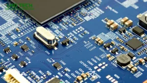
One of the most powerful techniques for enhancing signal quality is PCB back drill (or back drilling in PCB). This method specifically targets the hidden enemy of clean signals—via stubs—and helps reduce signal reflections, minimize loss and optimize circuit board performance. By selectively removing unused sections of drilled vias, back drilling offers a solution that extends beyond a single signal layer, benefiting the entire stackup in multi-layer PCB assemblies.
In this article, you’ll gain insight into how back drilling technology works, why it plays a crucial role in high-speed and high-frequency PCB design, and how you can use it to improve signal, reduce noise and ensure your latest PCB fabrication projects meet the highest standards for signal integrity and reliability.
PCB Back Drill Fundamentals

The PCB back drilling process is a secondary drilling procedure. This procedure is carried out after the initial via drilling and plating processes. The conventional drilling process creates through-holes that penetrate all layers. Not all vias require the use of the entire barrel structure. The unused portions on the barrel form via stubs. Signal operating frequencies continue to increase. Stubs cause severe degradation of signal quality during this process.
Back drilling is typically applied to selected vias after initial drilling to eliminate these copper stubs. By removing the extra via barrel (on either the entry side or the opposite side of the PCB), the back drill process creates a cleaner path for high-speed signals.
Back drilling offers several advantages:
- It reduces signal reflections that would otherwise bounce off the stub and cause data errors.
- It minimizes signal loss caused by impedance mismatches inside the via.
- It makes it possible to design high-speed and high-frequency PCBs while still using standard board stackups.
- It supports optimization in HDI designs and advanced applications.
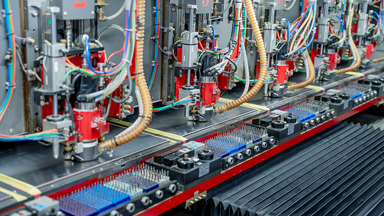
Back drilling is a drilling-based technique requiring precision CNC drilling machines for layer registration, careful depth control, and close coordination with fabricators during the PCB fabrication process.
Why Signal Integrity in PCB Design is Critical

An electrical signal transmits from the source end to the destination end. This process requires maintaining signal quality without degradation. Signal integrity in PCBs refers precisely to this characteristic. Circuit operating speeds continue to increase. The complexity of circuit design is growing daily. Maintaining signal integrity faces greater challenges. Once signal integrity is compromised, the bit error rate will rise. Timing issues arise as a result. Noise interference occurs in the data path. Electromagnetic compatibility tests may lead to failure.
The transmission process of high-speed signals imposes strict requirements on PCB design. The geometry of traces is one of the influencing factors. The specific structure of vias is equally critical. The arrangement of layer stackups cannot be ignored either. Minor discontinuities in the signal path may trigger reflection phenomena. Signal strength will consequently attenuate. Other nets may experience crosstalk interference. This ultimately manifests as a degradation in system performance.
Signal loss is proportional to both the length of the signal path and the number/characteristics of interfaces it crosses—including via transitions. Improving signal integrity is not just about wider traces or better materials, but about minimizing every possible source of discontinuity—including unused via stubs left after initial drilling.
Signal Integrity Challenges in Multi-Layer Circuit Boards
- Signal reflection caused by impedance mismatches in vias or at connectors.
- Crosstalk between adjacent nets due to improper routing or inadequate spacing.
- Signal degradation due to via stubs and inconsistent trace width.
- Variability in signal quality across large or stacked PCBs as signals travel through different layers.
Enhance signal integrity by targeting via stubs—which are among the most overlooked, yet most problematic, obstacles in high-speed and high-frequency applications.
Understanding Via Stubs and Signal Reflection
A via stub is the unused portion of a plated through-hole (PTH) via that doesn’t participate in the actual electrical path. When a drilled via connects, for example, only layers 2 and 5 of an 8-layer PCB, the remaining via length (from layers 1-2 and from 5-8) is not used and becomes a “stub.”
Why Are Via Stubs Problematic?
- A via stub acts as a tiny antenna, creating reflection points along the signal path.
- Signal reflection at via stubs leads to higher jitter, possible data loss and “eye diagram” closure.
- Stubs contribute to signal loss and degrade the integrity of high-speed signals in the signal layer.
- The longer the stub, the greater its impact—especially as frequencies and edge rates increase.
How Signal Travels Through a Via
As a signal travels through a via, any original via segments not immediately used can reflect part of the energy back toward the source. In essence, the via becomes a resonator, trapping and re-emitting energy at undesirable times, which causes signal degradation and can prevent signal from reaching its destination reliably.
Backdrilling in PCB is an elegant solution—by selectively removing the offending stub, the via is left with only the required connections, resulting in a cleaner signal and measurable improvement in PCB performance.
Back Drilling in PCB: How the Process Works
Step-by-Step Back Drilling Process
- Initial Drilling:After standard drill and copper plating, all vias are present in the PCB, including those with unnecessary tails.
- Identifying Critical Vias:Using signal integrity simulation and experience in the PCB industry, designers identify which vias are on high-speed signal paths and which need backdrilling based on signal integrity in high-speed.
- Controlled Depth Drilling:Controlled-depth drilling is performed on these targeted vias, using CNC machines programmed to remove only the unwanted segment of the via—measured from the entrance or exit side of the PCB.
- Cleaning and Inspection:Boards are cleaned to remove debris from the drilled stubs, then inspected for accuracy—using X-ray or microsection for position, back drill hole size and back drill depth tolerance.
Parameters for Optimizing Back Drilling
- Depth of the drill:Determined by the layer where you want to stop (the last connected layer).
- Back drill hole size:Typically, 0.05-0.10 mm larger than the original via for easy removal.
- Layer registration:Precise mapping between drill machine and layer locations is crucial to avoid damage to the PCB.
- Stub length:As short as possible, ideally below 0.3 mm for 10 GHz+ applications.
Back drilling technology plays multiple roles in circuit board manufacturing. This process is primarily used to eliminate via stubs. Impedance characteristics are optimized during this process. The signal path is thus maintained continuously. The entire transmission channel is therefore kept in an optimal working state.
Advantages: How Back Drilling Improves Signal Integrity
Back drilling offers several advantages that are especially important for high-speed and high-frequency PCB projects. Here’s how it works to enhance your designs:
1. Reduces Signal Loss and Signal Reflections
By physically removing via stubs, back drilling in PCB massively reduces points of impedance mismatch. This means:
- Lower signal reflection, which prevents destructive interference.
- Reduced insertion and return loss, making the board compliant with the latest data rate and communication standards.
- Cleaner and more reliable signal transmission along high-speed lines.
2. Improves Impedance Control
Impedance mismatches often occur where signals travel through a via stub—causing distortion. Back drilling technology removes the stub and helps maintain a constant impedance along the signal path, critical for maintaining signal integrity in high-speed PCBs.
3. Supports Higher Speed and Frequency
Modern protocols like 56G PAM4, 100G Ethernet, and high-frequency RF require ultra-clean channels. PCB back drill enables these rates by minimizing stub effects, which would otherwise make such speeds impossible on typical stackups.
4. Boosts Overall Signal Quality and Reliability
- Enhances signal integrity for both point-to-point and bus-based designs.
- Reduces EMI and crosstalk by eliminating copper stubs as unintended antennas.
- Provides better signal integrity simulation results, closing the gap between modeling and real-world measurements.
5. Enables Denser, More Flexible PCB Design
Back drilling technology allows designs to incorporate more layers. Interlayer stacking density is thereby increased. Signal quality remains unaffected during this process. HDI designs, where vertical routing is unavoidable, thus receive critical support. Multi-board assembly scenarios also benefit from this technology.
Industry Applications: Why High-Speed and High-Frequency PCB Design Relies on Back Drilling

In the field of PCB manufacturing, back drilling has become a necessary process. This method is required for any design involving high-speed or low-loss data transmission. The core application areas of this technology include the following categories.
- Telecommunications:Switches, routers and backplane boards for data centers and ISPs trust back drilling to minimize signal loss at 28+ GHz.
- 5G and RF Communications:Transceivers, base stations and mmWave devices require ultra-low stub lengths for clean signal propagation.
- Consumer Electronics:High-speed memory buses, display interfaces and processor-to-processor links in laptops, gaming and mobile devices.
- Automotive Electronics:ADAS, infotainment and radar systems use back drilling to maintain signal integrity and reliability under shock or vibration.
- Aerospace/Defense:Signal reliability under extreme conditions requires stub-free channels to avoid mission failure.
- Medical Devices:Imaging, monitoring, and critical diagnostic gear benefit from reduced signal noise and minimal data errors.
PCB fabrication for these industries often relies on controlled-depth drilling and back drilling technology as standard manufacturing steps.
Back Drilling vs. Other Drilling-Based Technologies
While back drilling offers several advantages for signal clarity, it is not the only drilling-based strategy for optimizing vias:
| Technology | Stub Removal | Density | Cost | Best Use Case |
| Back drilling | Excellent | Med-High | Moderate | High-speed, high-frequency, HDI, upgrade legacy boards |
| Blind/Buried vias | Excellent | Very High | High | Ultra-dense HDI, BGA, advanced consumer/AI/IoT |
| Microvias (laser) | Best | Ultra High | Very High | BGA/cellular modules, extremely small form-factor designs |
| Standard TH vias | Poor | Med | Low | Power, ground, low-speed boards |
Back drilling is typically chosen where maximum signal integrity is needed but at a more manageable cost and process complexity compared to laser-processed vias.
Design Best Practices to Enhance Signal Integrity
Optimizing your PCB design for back drilling and high-speed signals requires careful planning:
- Identify High-Speed Signal Paths:Use EDA simulation and SI analysis to mark all critical nets where back drilling will improve impedance and minimize signal loss.
- Minimize Unnecessary Vias:Every via introduces noise potential. Use only the required vias and select only those with meaningful stub lengths for back drilling.
- Control Drill Depths and Hole Sizes:Ensure that your controlled-depth drilling process won’t accidentally break through active layers or create excessive clearances.
- Maintain Consistent Signal Path:Route traces to keep impedance as uniform as possible across both traces and drilled vias—use curves instead of right-angles where feasible.
- Inspect and Document:Include test coupons for cross-section; record all back drill locations, hole diameters and layer stops in your fab documentation.
- Work Closely with Your Fabricator:Share your signal integrity simulation models and back drilling requirements for optimal manufacturability and performance.
Advanced Techniques and Practical Examples
Back drilling can significantly improve not just a single net but the overall electromagnetic environment inside the PCB. Here’s how advanced teams leverage the technology:
Simulation and Measurement
- TDR (Time Domain Reflectometer) Analysis:Used both in simulation and on-tested boards, TDR helps visualize the reduction in stub-related reflection after back drilling.
- S-Parameter Extraction:SI engineers use before-and-after S-parameter data to quantify decreased insertion loss.
Challenges in PCB Back Drilling and Solutions
Despite its benefits, challenges in PCB back drilling remain:
- Depth Accuracy:The deeper the multi-layer board, the tighter the depth tolerance required. Advanced CNC and registration systems are a must.
- Yield Risk:Poorly executed backdrilling can lead to incomplete stub removal or even damage to the signal layer, which can degrade signal or cause open circuits.
- Cost:Additional drill passes, inspection and process controls increase the per-board cost—justified only for high-speed and high-frequency applications.
- Documentation and Communication:Ambiguity in design files or miscommunication with fabrication partners remains a leading cause of manufacturing defects.
The Future of Back Drilling Technology in PCB Manufacturing
With the drive to 56G/112G Ethernet, Wi-Fi 7, and 5G/6G, back drilling plays a crucial role in enabling new standards. The future promises:
- Increased Automation:AI-driven design tools automatically select and specify back drill candidates based on signal integrity simulation outputs.
- Greater Accessibility:More fabricators now offer controlled-depth drilling as a standard service, making advanced signal integrity attainable for mid-size production runs.
- Integration with Other Technologies:Combining laser-drilled microvias, via filling, and back drilling enables even denser and more reliable PCB designs—especially for IoT and AI modules.
Back drilling is a powerful tool that will remain central to PCB design and manufacturing for years to come, especially as board complexity and data rates increase.
FAQs: PCB Back Drill, Signal Loss and Manufacturing
Q: Why does back drilling selectively remove via stubs and not all vias?
A: Not all vias cause meaningful signal degradation. Only those carrying high-speed, critical signals—and where stub length exceeds recommended limits—require back drilling based on signal integrity simulations.
Q: Can back drilling damage the PCB or signal layer?
A: Improper depth control during controlled-depth drilling can cause damage to the PCB, but with precise registration and experienced fabrication, risks are minimized.
Q: Does back drilling improve every kind of signal?
A: Back drilling improves signal integrity for high-speed and high-frequency signals, but low-speed or static nets (like power/ground) do not benefit significantly.
Q: How do I specify which side of the PCB or opposite side for drilling?
A: Your layer stackup drawing should indicate which side the signal travels from and to, and the drill depth should be referenced from the relevant side in your fab documentation.
Q: What role does back drilling play in high-speed PCB design upgrades?
A: If your board was designed for lower speed but needs to be repurposed for higher-speed applications (such as upgrading from 10G to 25G or 56G data rates), back drilling offers several advantages. You can retrofit legacy designs by performing back drilling on critical vias, greatly reducing signal loss and reflection without redesigning the entire stackup. This approach allows you to maintain signal integrity in PCB upgrades and support modern protocols cost-effectively.
Q: What is the ideal stub length after back drilling for high-frequency PCB?
A: For high-speed and high-frequency PCB applications, the residual stub length should ideally be less than 0.3mm. In 56G and 112G designs, some engineers target even shorter lengths (<0.1mm) to minimize impedance discontinuities and ensure cleaner signals.
Q: How is back drill depth tolerance controlled?
A: Precision CNC drilling equipment is programmed using CAM data directly derived from your design files. Depth is closely monitored and verified using cross-section testing, X-ray imaging, and real-time sensors to ensure back drill depth tolerance stays within tight limits and avoids potential damage to the PCB.
Q: Is back drilling suitable for every PCB fabrication project?
A: While beneficial for high-speed signal and high-frequency signal transmission, back drilling is best reserved for applications where signal loss, signal reflection and signal integrity are critical deliverables. Routine consumer or low-frequency boards may not need backdrilling as a cost-saving measure.
Conclusion: Why Back Drilling Offers Several Advantages for Signal Integrity
Back drilling in PCB design is more than just a manufacturing step—it’s a strategic solution to one of the most challenging aspects of high-speed PCB design: maintaining signal integrity. As signal travels through high-density, multi-layer circuit boards, even small via stubs can cause disproportionate harm in the form of signal reflection, signal loss and signal degradation.
Back drilling technology selectively removes those via stubs through controlled-depth drilling, providing:
- Cleaner, more reliable high-speed signal transmission
- Reduced signal loss and minimized reflection
- Enhanced signal quality and easier compliance with industry standards
- Flexibility to upgrade products without full redesigns
- Support for high-speed and high-frequency applications in telecommunications, data centers, automotive, aerospace and beyond
Back drilling is essential in today’s PCB industry for those seeking to optimize signal performance, minimize signal distortion, and future-proof circuit boards for emerging standards. By partnering with experienced fabricators, leveraging advanced EDA tools, and adhering to best practices for documentation and testing, you can ensure your design achieves its signal integrity, reliability and speed targets.
No matter how advanced your next printed circuit board may be, if maintaining signal integrity in high-speed designs is a priority, back drilling plays a crucial role. The technique will remain at the forefront of innovation as the need for high-speed data, reliable communication and dense board layouts continues to rise.