
Introduction: What is PCB Assembly?

PCBA refers to the complete process of mounting electronic components onto a printed circuit board. This process transforms a bare board into a fully functional circuit board that performs specific electronic functions—namely, a PCB that has completed its assembly steps. This assembly process holds a central position in the electronics manufacturing industry. The technique brings any designed circuit to life, evolving it from a paper blueprint into a physical entity, thereby powering everything from mobile phones to advanced medical devices.
Assembly methods have undergone rapid evolution. Current PCBA processes integrate automated steps with manual operations, resulting in each electronic component being precisely placed onto the circuit board and forming reliable connections. This PCBA guide breaks down each phase step by step, helping readers understand the complete journey from the schematic on the design drawings to the final operational assembled board.
Printed Circuit Boards & PCB Assemblies: The Backbone of Modern Electronics
Printed circuit boards provide the functions of supporting electronic components, connecting circuits and layout arrangement. Manufactured with a multi-layer structure, the internal copper foil circuits form a precise interconnection network, replacing traditional wiring harnesses. Subsequent assembly processes mount and solder electronic components onto the printed circuit board, turning non-functional bare boards into functional units. This assembly step is the core process.
Why PCB Assembly Is Essential
- Functionality: The assembly process play is vital for any device, as only after all PCB components are soldered in place will the board function as designed.
- Reproducibility: Modern electronics manufacturing employs both automated assembly processes and manual assembly processes. The combination of these two techniques enables the manufacturing process to achieve stable quality in quick-turn PCBA or mixed-volume production, with repeatable results.
Understanding the PCB Assembly Process
A robust guide to PCB assembly covers everything from designing the circuit to the final inspection of the finished board. The PCBA process consists of several stages:
- Preparation and DFM (Design for Manufacturability) review
- Solder paste application
- Component placement (Pick and Place)
- Soldering process (Reflow or Wave Soldering)
- Inspection and Quality Assurance
- Through-hole and mixed assembly processes
- Final inspection, testing, and finishing
LHD TECH’S Key Steps in the PCB Assembly Process
Solder Paste Application

The first step in SMT assembly applies solder paste onto the corresponding pads on the PCB surface. Solder paste is a material composed of fine solder particles mixed with flux. Operators or equipment use a stencil to precisely print the solder paste onto every soldering point for surface mount components. The precision of this printing step determines the connection quality of the subsequent solder joints.
Pick and Place Process

During the mounting process, components are placed directly onto the printed circuit board pre-applied with solder paste. Modern electronic assembly lines adopt high-speed pick-and-place machines, which mount thousands of SMD components per hour with extremely precise placement for each component. The production of prototype boards or special-specification boards relies on manual mounting. This process ensures that fragile or odd-shaped components are correctly installed.
- Key Point: The automated placement process can handle mixed assembly of various components, including tiny resistors and complex processors. This process enhances PCBA production efficiency while maintaining placement accuracy.
Reflow Process

The assembled circuit board enters the reflow oven. The temperature inside the oven rises gradually according to a preset profile, and the solder paste melts to form electrical connections between the pads and component leads. The circuit board is then cooled, and all surface-mounted components are securely soldered. This process permanently attaches electronic components to the printed circuit board.
Inspection and Quality Control

There is no room for compromise on quality requirements. Following the reflow soldering process, automated optical inspection (AOI) equipment verifies component placement and solder joint quality, detecting defects such as misalignment or missing components. For high-density integrated circuits, such as BGA-packaged chips, X-ray inspection ensures that hidden solder joints are free of defects. Final inspection and in-circuit functional testing together ensure that the assembled boards achieve perfect performance.
Common Inspection Methods
| Inspection Type | Used For | Benefit |
| Visual | Gross defects, prototyping | Quick, cost-effective |
| AOI | SMT mass production | Rapid, identifies subtle defects |
| X-ray | BGAs, hidden joints | Reveals hidden solder issues |
| Functional | Board-level testing | Confirms circuit functionality |
Through-Hole Insertion and Soldering

Not all components are surface-mount; some require through-hole insertion. In this process, leads are placed into holes on the PCB board and soldered—either by hand (for low quantity or sensitive circuits) or via wave soldering (for high-volume runs). Through-hole assembly increases mechanical strength, vital in power electronics, connectors or high-stress assemblies.
Final Inspection

After both SMT and through-hole, a thorough final inspection is conducted. Boards are checked for solder bridges, misplaced components, open circuits and cosmetic quality—a necessary step before cleaning and finishing.
Cleaning, Coating and Packaging

Residues from soldering must be removed (especially in high-reliability or medical electronics), using deionized water, solvents or ultrasonic cleaning. Conformal coating or potting is sometimes applied for moisture and dust resistance. Finished PCB assemblies are packaged in ESD-safe bags for shipment.
LHD TECH’S Types of PCB Assembly Methods: SMT, Through-Hole and Mixed Assembly
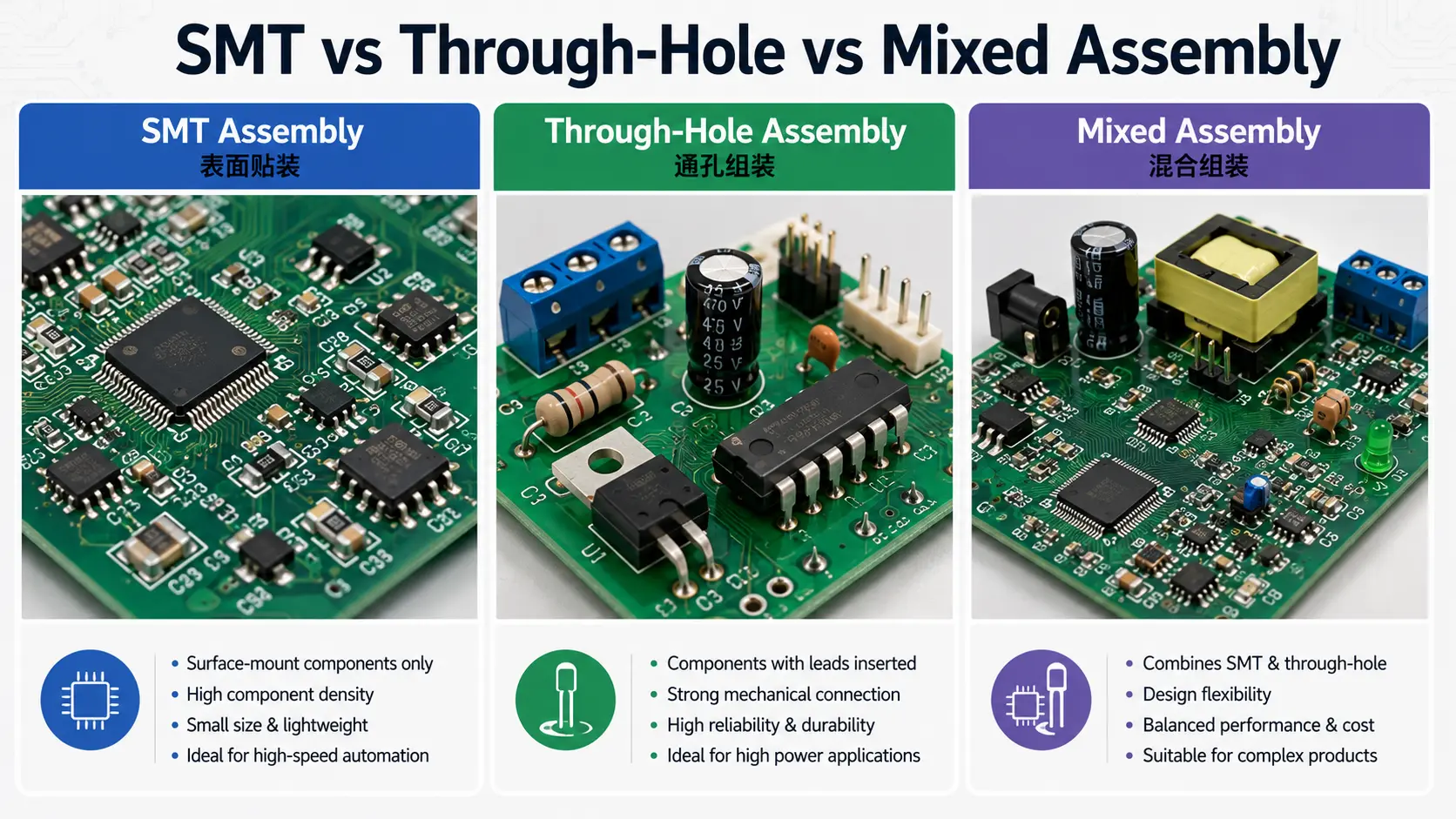
SMT Assembly
Surface mount technology (SMT) is the most widely used technology in the field of electronics manufacturing. This process places components on the surface of a PCB and secures them through reflow soldering. SMT enables the assembly process to be automated, achieving high speed and high repeatability.
Through-Hole Assembly
Through-hole assembly technology inserts component leads into pre-drilled holes on a printed circuit board; soldering and fixing of the leads is completed on the opposite side of the board. This assembly method creates a high mechanical bond strength, making it suitable for circuit applications demanding stringent structural strength and reliability: power modules, connector assemblies, industrial control systems and automotive electronic systems.
- Through-hole PCB assembly process is especially popular for prototype builds, fields requiring high reliability or where future rework might be likely.
- Use automated insertion equipment for large runs, and manual assembly for small-batch or specialty designs.
Mixed Assembly
Mixed assembly combines both surface mount technology (SMT) and through-hole assembly on the same pcb board. This process lets designers deploy the strengths of both approaches on a single assembled PCB—for example, mounting chips and passives via SMT, while using through-hole methods for connectors, transformers or bulky board components.
- A typical mixed assembly efficient pcb will use SMT for high-density logic and through-hole for power or mechanical connections.
- Coordinate with your assembly partner early. Mixed assembly processes require careful sequencing to ensure that board components do not interfere with soldering process flows.
Comparing PCB Assembly Methods
| Assembly Method | Common Use Cases | Pros | Cons |
| SMT | Consumer, telecom, IoT | Compact, automated, high-speed | Less robust for stress |
| Through-Hole | Power, connectors, relays | Robust, easy for prototyping | Slower, less automated |
| Mixed Assembly | Automotive, industrial | Versatile, best of both worlds | Requires coordination |
Key Files and Data for LHD TECH’S PCB Manufacturing and Assembly

Successful electronic manufacturing hinges on thorough, accurate documentation. Before the assembly process consists of several key data sets:
- Gerber Files: Outline every copper layer, drill locations, solder mask openings and board outline for the bare PCB.
- Bill of Materials (BOM): Lists each electronic component, describing footprints, supplier part numbers and approval status for equivalents (helpful if components are out of stock).
- Pick and Place File (Centroid): Details X/Y locations, rotation and layer (top/bottom) for where components are placed on top of the board.
- Assembly Drawings: Visual workflow for assembly personnel, specifying component orientation, noting sensitive parts and highlighting unique board features.
Component Selection & Sourcing in Electronic Manufacturing

Component availability is one factor, and supply chain strategy is another. These two factors together determine PCBA cost. Modern electronics manufacturers rely on a global network, sourcing various components through this network, including resistors, capacitors, integrated circuits, connectors and specialty chips.
- During the circuit board design phase, multi-sourced components should be selected. These components must be supported by global distributors. This approach helps avoid the emergence of supply bottlenecks.
- Add alternate supplier part numbers for critical components in your BOM to speed up the assembly process and maintain production during shortages.
Case Study:
A wearable device startup used only one temperature sensor vendor in their BOM. When COVID lockdowns froze production at that vendor’s factory, the assembly line halted for two months. Adding multiple approved alternates in future builds ensured their next quick-turn PCB assembly went uninterrupted.
Challenges and Solutions in PCB Assembly
PCB assemblies confront many hurdles, from design issues to assembly process errors:
| Challenge | Solution |
| Solder bridges | DFM checks, correct stencil design, AOI, proper solder paste volumes |
| Misplaced PCB components | High-precision pick and place process, thorough documentation |
| Warped circuit boards | Use thicker substrate, balance copper, proper handling during reflow process |
| Missing board components | Automated optical inspection, cross-check BOM/pick-and-place output |
| Cold solder joints | Fine-tuned soldering process, validated reflow temps, clean leads/pads |
| Availability of components | Pre-authorized alternates, design for supply chain, early sourcing |
- Quality Assurance: The production process involves both manual inspection and automated inspection methods. Inspection equipment performs Automated Optical Inspection (AOI), X-ray inspection and functional testing procedures. These procedures identify potential issues before the circuit boards are delivered in the final product.
- Design for Manufacturability (DFM): Early review lowers defects, reduces cost and speeds up the entire assembly process.
LHD TECH’S Cost of PCB Assembly and Efficiency Tips

The cost of PCB assembly isn’t just about the price of each component—it’s also about manufacture and assembly complexity, labor and processing steps. Here’s how to keep your costs in check:
- Standardize footprints: Use common SMD sizes so that pick and place setup is streamlined.
- Batch orders: Higher volume lowers per-unit costs in most assembly processes.
- Early DFM: Prevents expensive rework or mistakes at the previous steps of the assembly process.
- Prototype runs: Validate designs before committing to mass production; issues caught early save time and money.
Cost Levers in PCB Solutions
| Cost Driver | Potential Impact | Mitigation Strategy |
| Batch size | High | Aggregate orders |
| Unique part count | Moderate | Consolidate, share footprints |
| Hand assembly vs automation | High | Automate when feasible |
| Double-sided assembly | Moderate | Group on one side if possible |
| Test & inspection depth | Variable | Use risk-based approach |
- Efficient PCB assembly uses panelization, minimizes board size, reduces hand steps and clearly communicates requirements to production.
How to Choose the Best PCB Assembly Partner

Choosing LHD TECH as your PCBA partner can determine your product’s success:
- Look for: You benefit from LHD’s IPC, RoHS and ISO certifications; mixed assembly capabilities; quick-turn options; and robust quality assurance including final inspection protocols.
- Evaluate: You can count on LHD’s engineering support (DFM/rework assistance), flexible minimum order quantities, and transparent cost and schedule communication.
- Ask for references: You will find that LHD has successfully completed similar projects in your sector among its previous assembled PCB work.
- Prototype service: You gain access to both prototype and volume production services, ensuring you can scale quickly once your design is locked.
Trends and Innovations in Modern Electronics Manufacturing
- Automation & Smart Factories: Real-time monitoring, AI-powered defect detection, and flexible robotic assembly processes enable both high volume and custom runs.
- Miniaturization: Efficient PCB designs are more compact, using microvias, high-density interconnect (HDI) and advanced materials.
- Green Techniques: Lead-free solder, recyclable packaging and eco-friendly board chemistries are now industry standards.
- Distributed Manufacturing: Quick-turn assembly and regional PCB solutions mean less shipping time, local sourcing of components and easier scaling from prototype to mass production.
Conclusion: Your Path to Efficient, Reliable PCB Assemblies
PCBA is central to every successful electronic product, from prototype to mass production. Mastering the full process—from solder paste to final inspection—creates reliable, cost-effective, and innovative products that excel in today’s competitive electronics manufacturing environment.
Mastering SMT and through-hole assembly, with adaptable processes and strict quality control, ensures maximum precision in placement, soldering and testing. Combined with rigorous documentation, strategic procurement, efficient design and strong partnerships, this delivers reliable PCB solutions.
The PCBA process includes DFM review, stencil printing, pick-and-place, reflow or wave soldering, AOI and X-ray inspection, cleaning and final inspection before the board leaves the line. Whether for cutting-edge IoT devices, automotive control systems, or medical wearables, investment in a comprehensive, reliable PCBA process pays off in customer satisfaction, minimized field failures and lasting brand trust.
Key takeaways for success in modern electronics manufacturing:
- Invest in DFM and DFA reviews to ensure efficient and cost-effective assembly.
- Keep all files, from your bare PCB Gerber layouts to your BOMs and assembly drawings, up-to-date and error-free.
- Use prototype runs for validation before full production to catch any assembly process hiccups.
- Select assembly partners who prioritize quality—look for IPC certification, multi-technology assembly capabilities, and strong communication.
- Balance speed, flexibility and reliability to optimize the cost of PCB assembly over the entire product lifecycle.
Final Words
By following this extensive guide to PCB assembly, embracing best practices in SMT, through-hole, and mixed assembly methods, and utilizing both automated and manual procedures, you’re set to maximize your team’s efficiency, the reliability of your electronic assembly, and the overall performance of your final product. Efficient PCB design, thorough process control, and effective collaboration with your assembly partner are the linchpins of modern electronics manufacturing.
Whether it’s your first prototype or your millionth production batch, a deep understanding of the full PCB assembly process ensures your circuit boards will not only function as intended, but also excel in the field for years to come.