
Introduction to Acceptance Criteria for PCBs
Innovative design and advanced assembly lines do not determine the fundamental nature of equipment. The core foundation of high-quality electronic equipment lies in the reliability of printed circuit boards.Market competition in the electronics industry is extremely fierce. Minor defects in printed circuit board manufacturing can lead to large-scale product recalls, customer dissatisfaction and potential safety hazards.Enterprises clearly formulate and strictly implement acceptance criteria, which are the core of quality and reliability assurance systems.
Acceptance criteria are far more than just a piece of paperwork.This system includes standards, inspection methods and acceptance benchmarks. These multiple dimensions work together to ensure that reliability-compliant printed circuit boards proceed to the assembly stage.Enterprises can establish control specifications based on globally recognized industry standards such as IPC-A-600 issued by the Association Connecting Electronics Industries (IPC).These standards guide engineers to identify and control production defects, achieve continuous optimization of production processes and minimize the risk of product failure in actual applications.
What Are Acceptance Criteria for PCBs?
Acceptance criteria define the qualification threshold for each circuit board from three dimensions: physical properties must meet requirements, electrical performance must be qualified and appearance quality must comply with specifications.This complete set of requirements ensures that every printed circuit board not only meets the specific parameters put forward by customers, but also meets the industry’s basic expectations for product quality and long-term reliability.
Key acceptance criteria for PCBs often include:
- Dimensions and Tight Tolerances: Ensuring that the board’s thickness, outline, and hole sizes align precisely with design files. Even a minor deviation can disrupt component alignment during assembly.
- Copper Plating: Traces and vias must achieve adequate copper thickness. This parameter directly determines whether their current-carrying capacity and mechanical strength meet requirements. For Class 3 boards—products used in high-reliability applications—the sufficiency of copper thickness is even more critical.
- Solder Mask Coverage: The solder mask should protect copper areas not meant to be soldered, preventing shorts and leakage.
- Silkscreen and Markings: All printed identifiers should be clear, legible, and stable to ease the assembly and inspection stages.
- Conductivity: 100% electrical testing for continuity and isolation ensures that there are no shorts, opens, or power integrity issues.
LHDPCB’S Key Criterion for PCB Acceptance
To manufacture high-quality printed circuit boards (PCBs), LHDPCB must not only meet all criteria listed in the inspection checklist but also exceed these basic requirements.Listed below are examples of critical acceptance standards that comply with the IPC-A-600 PCB inspection specification.
| Criterion | Acceptance Standards (Common) | Linked Performance Class |
| PCB Dimensions | ±0.13mm from design | Class 2, Class 3 |
| PCB Thickness | As per stack-up, ±0.1mm | Class 2, Class 3 |
| Copper Plating | ≥20μm (Class 2), ≥25μm (Class 3) | IPC-A-600, IPC-6012D |
| Solder Mask | No voids/wrinkles, tight coverage | IPC-A-600, Class 2/3 |
| Via/Hole Size | ±0.05mm from design | IPC-A-600, Class 2/3 |
| Silkscreen Legibility | Clear, no smears, accurate | IPC-A-600, All Classes |
| Foreign Inclusions | None on surface or internal | IPC-A-600, Class 2/3 |
| Conductor Spacing | Within specified PCB DRC limits | IPC-A-600, IPC-2221 |
| Plated-Through Holes | Proper plating, no blockages | IPC-A-600, All Classes |
| Surface Finish Quality | Uniform, no oxidation or scratches | IPC-A-600, All Classes |
| Power/Impedance Control | As spec’d, ±10% (RF/5G PCBs) | Class 2/3, HDI/Rogers/Flex PBCs |
IPC-A-600: The Standard for PCB Quality
The gold standard for acceptance criteria in the pcb industry is the IPC-A-600 standard. Established by the Association Connecting Electronics Industries (IPC), this comprehensive guideline spells out visual and dimensional acceptance requirements, class by class.
Why is IPC-A-600 So Important?
- Universal Alignment: IPC standards establish a unified industry language, allowing the procurement department, engineering and technical personnel, and the assembly line to form consistent judgment criteria for “qualified” products throughout the entire production chain.
- External and Internal Guidelines: Covers everything from visible surface defects to micro-sectioned internal layers and plated-through holes.
- Photographic Visual References: Hundreds of photos show actual examples of acceptable and defect conditions—a boon for training and auditing.
- Foundation for Class 2 and Class 3 Board Standards: This standard establishes clear acceptance requirements for different application classes. It establishes basic criteria for general electronics (Class 1). It sets a higher threshold for dedicated service products (Class 2). It imposes the strictest requirements for high-reliability applications (Class 3).
IPC-A-600 plays a central role in the procurement process and quality assurance system.This standard is commonly used together with IPC-6012D (Specification for Rigid Printed Boards) and IPC-6013C (Specification for Flexible Printed Boards).The three standards are interconnected and form a complete normative framework for the procurement, acceptance and quality control of printed circuit boards.
LHDPCB’S Classes of Acceptability: Class 2 and Class 3 PCB Boards

IPC-A-600 divides circuit boards into performance classes, each with its own tier of acceptability requirements:
- Class 2 (Dedicated Service Electronic Products): Used in most industrial and commercial electronic manufacturing. Class 2 boards must meet stringent standards for workmanship and function but allow minor visual imperfection if it doesn’t impact service life or reliability.
- Class 3 (High-Reliability Electronic Products): Class 3 boards require the tightest tolerances and most exhaustive inspection.Class 3 printed circuit boards are dedicated to mission‑critical electronic equipment.Medical devices, aerospace control systems and military electronic equipment all fall into this category of applications.Any minor manufacturing defects are deemed unacceptable in these fields.Class 3 PCBs must meet the most stringent tolerance standards, and their production process requires the most comprehensive inspection procedures.
Key Differences Between Class 2 and Class 3 PCBs
| Feature | Class 2 (Standard for PCB) | Class 3 (Stringent for PCB) |
| Visual Defects | Some minor allowed | None allowed |
| Copper Thickness | ≥20μm | ≥25μm |
| Solder Mask Voids | Minor outside pads allowed | None allowed |
| Warpage | <0.75% board diagonal | <0.5% of board diagonal |
| Foreign Inclusions | Almost none permitted | Absolutely none permitted |
| Application | Industry/Consumer | Aerospace/Medical/Military |
Critical Acceptance Requirements According to Industry Standards

To conform to industry standards, every pcb must meet acceptance standards at three key checkpoints:
1. External Features (Surface Level)
- Copper Trace Width/Spacing: Must match Gerber design files; conductor spacing is critical for both low and high-voltage PCBs.
- Solder Mask Quality: Solder mask coverage ensures no leakage or shorting, protecting circuitry during both use and pcb assembly.
- Board Edge Quality: Edges must be smooth, free of burrs or delamination and meet V-CUT and panelization requirements.
2. Internal Features (Plated-Through Holes, Layers & Material)
- Plated-Through Holes (PTHs): The plating must form a uniform coating on the inner walls of through‑holes without any manufacturing defects, and must adhere firmly to the inner layers of the hole wall.Insufficient plating thickness, cracks or voids on the hole wall can lead to intermittent circuit interruptions and degraded performance. Such problems are particularly prone to causing system failures in high‑current or signal vias.
- Internal Layers and Inclusion: Cross-sectional analysis must show no delamination, misregistration, or foreign inclusions (like dust or resin pockets) between layers. This is non-negotiable for Class 3 boards.
- Dielectric and Lamination Quality: Insulating laminates must undergo strict inspection after manufacture.No bubbles, voids or embedded particles shall be present inside the material.If such microscopic defects are not removed, they will develop into insulation failure points during long-term operation and eventually lead to dielectric breakdown or surface arcing failures.
- Conductor Spacing: Even internally, traces must maintain minimum spacing per design and IPC guidelines to avoid shorts and leakage, especially under high voltage.
3. Environmental Resistance & Long-Term Reliability
- Solderability: All exposed copper pads and features must accept solder smoothly without flux residues, discoloration or oxidation.
- Surface Finish Durability: Finishes such as ENIG or OSP must withstand assembly and end-use conditions without flaking or causing solder “de-wetting.”
- Strain and Flexure: Rigid-flex and flexible PCBs must survive repeated bends without cracking traces or detaching coverlay.
LHDPCB’S Inspection Methods in the PCB Manufacturing Process
Rigorous inspection is vital for detecting defects and maintaining consistent quality in pcb production. Here’s how modern facilities inspect every criterion:
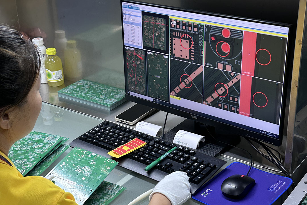
Visual Inspection
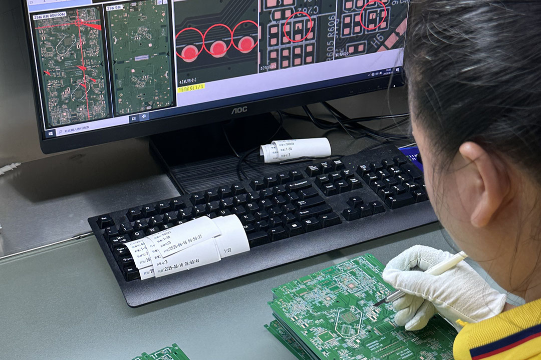
- Automated Optical Inspection (AOI): Scans each board to detect flaws in trace width, solder mask, silkscreen alignment, and surface contamination. AOI is the core of high-volume electronic manufacturing.
- Manual Visual Inspection: IPC-trained inspectors use magnification to check for surface defects, pad lifting, and solder mask coverage.
- Lighting & Magnification: Strong, even lighting and magnifiers of at least 5x to 30x for critical regions.
Electrical Testing

- Flying Probe Testing: Used for prototyping or low-to-medium volume; probes move across all nets to ensure full continuity and isolation.
- Bed of Nails: Standard for high-volume production: custom fixture with pins for simultaneous multi-net testing. Provides full coverage and rapid throughput.
Microsection and X-Ray Analysis
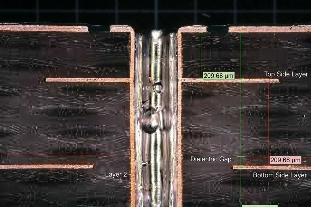
- Microsectioning: Destructive analysis on sample PCBs to inspect internal barrel plating, via wall quality, and inclusion of foreign objects. Results are benchmarked against IPC-A-600.
- X-ray Inspection: Especially valuable for complex multilayer, HDI and BGA PCBs, detecting internal defects and voids invisible at the surface.
Statistical Process Control (SPC)

- SPC Charts: Used throughout the manufacturing process (plating thickness, hole alignment, solder mask registration) to spot out-of-control trends and prevent escapes.
- Data-Driven Quality Assurance: Automatic data capture from AOI, electrical, and SPC systems allows manufacturers and engineers to refine processes and raise yield rates.
Managing Acceptance Criteria for Different PCB Types
Different technologies have unique criteria in the PCB industry:
| PCB Type | Special Criterion/Focus |
| Rigid PCB | Warpage, copper adhesion, PTH integrity |
| Flex & Rigid-Flex | Bend radius conformity, coverlay adhesion, cracked conductors |
| HDI PCB | Microvia integrity, fine conductor spacing, precise stackup |
| Aluminum/IMS PCB | Dielectric uniformity, aluminum-copper bond, thermal cycling |
| Rogers PCB | Dielectric constant uniformity, low-loss, surface finish |
Quality Assurance and Statistical Process Control in PCB Production

LHDPCB integrate robust quality assurance and statistical process control into every phase:
- In-Process SPC: Real-time monitoring during plating, lamination, and drilling to maintain tight tolerances.
- Workmanship Training: IPC-trained operators and inspectors are crucial to consistent application of acceptance standards throughout the manufacturing process.
- Data Traceability: Every PCB lot receives a unique batch number linked to process data, electrical test results, and microsection images. Essential for regulatory compliance in medical, avionics, and military sectors.
Common Defects, Foreign Inclusions and Imperfections in PCBs
Despite best efforts, PCB production can yield the occasional defect. Here are the most common issues and why they’re unacceptable under industry standards:
| Defect Type | Description | Impact |
| Foreign Inclusions | Dust, fibers, or metal embedded in laminate or traces | Can cause shorts, breakdown, arcing |
| Pad Lifting | Copper pad detaching from substrate | Leads to open circuits |
| Solder Mask Voids | Areas of missing or thin mask on critical copper | Risk of shorts, corrosion, leakage |
| Barrel Cracks | Cracks in via/barrel wall plating | Unreliable interconnection |
| Copper Thinning | Etched traces or barrels below minimum thickness | Poor current capacity, risk of burnout |
| Conductor Spacing Violation | Traces too close together | Short circuits, electrical leakage |
| Delamination | Separation of board layers, visible as bubbles or blisters | Insulation failure, mechanical weak |
| Warpage | Excessive bow/twist of finished board | Assembly issues, stress on solder |
Procurement and Documentation Best Practices
Engineers and purchasing professionals should:
- Specify acceptance criteria and IPC class (e.g., Class 2 or Class 3) in every order and fabrication drawing.
- Request all inspection records: electrical test reports, AOI images and microsection certificates for every lot.
- Audit suppliers: Visit or request a quality audit before large-scale procurement. Ensure process control is as rigorous as the acceptance criteria themselves.
- Maintain clear communication channels: Early alignment reduces disputes, speeds up time-to-market and facilitates rapid problem-solving if an issue does arise.
Checklist:
- Defined PCB acceptance criteria and class for each design
- Shared all Gerber, stackup, and drill data with fabricator
- Collected inspection data and certificates for each batch
- Conducted periodic supplier audits
- Updated documentation as standards evolve
Conclusion: Ensuring Reliable Electronics Through Stringent PCB Acceptance Criteria
The electronics industry is currently in a phase of rapid development. We must ensure that every stage of printed circuit board design, manufacturing, and procurement strictly meets acceptance standards. Only by adopting the IPC-A-600 standard, accurately distinguishing between the different standards for Class 2 and Class 3 products, and establishing a rigorous process control system can we gradually build a quality system and ensure reliability.
By inspecting for every criterion and rejecting any imperfection that threatens product performance, you ensure reliable circuit boards form the heart of your electronic devices. Whether you’re producing consumer gadgets or mission-critical systems, stringent acceptance standards aren’t just about compliance—they’re your ticket to market leadership and customer trust.
If you’re ready to raise your PCB quality to the next level, start with clear acceptance criteria, partner with proactive IPC-certified manufacturers like LHDPCB, and always verify every batch before it goes to assembly. That’s how you transform diligence into enduring market advantage.