
Introduction
LHD TECH has been deeply involved in the PCB manufacturing or PCB assembly industry for many years. Every day, we come into contact with a large number of engineers who are meticulous about the manufacturing process. During the communication with them, we found that even experienced professionals often get confused about the two core concepts of “solder mask layer” and “paste mask layer”. Today, we will analyze the core differences and key roles of the two in a simple and clear way.
In the entire process of PCBA (Printed Circuit Board Assembly) and PCB manufacturing, accurately understanding and applying these two types of masks is the cornerstone for ensuring product yield and reliability. Whether it’s rapid prototyping or high-difficulty batch PCBA services for automotive electronics, aerospace, consumer electronics and other fields, we believe that the ultimate control over process details is the only way to deliver zero-defect products.
First, let’s focus on Solder Mask – the Solder Mask.
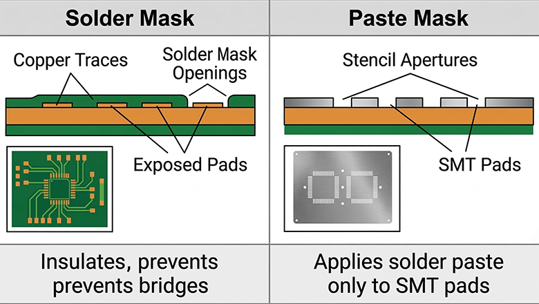
- The solder mask, commonly known as “green oil”, is a permanent protective coating covering the surface of a PCB. In the manufacturing standards of PCBS, solder mask shoulders three core missions:
- Physical protection: Isolate the copper foil circuits from the air to prevent oxidation and ensure the long-term stability of electrical connections.
- Process isolation: During wave soldering or reflow soldering, it prevents short circuits caused by bridging between adjacent solder joints. This layer of “insulating barrier” is the prerequisite for achieving high-density wiring.
- Precise window opening: The solder mask layer will be “opened” on the pads that need to be soldered or the test points that need to be touched through a pattern transfer process, exposing the copper surface below (usually requiring surface treatment), while the other areas are tightly covered.
What is a Solder Mask?
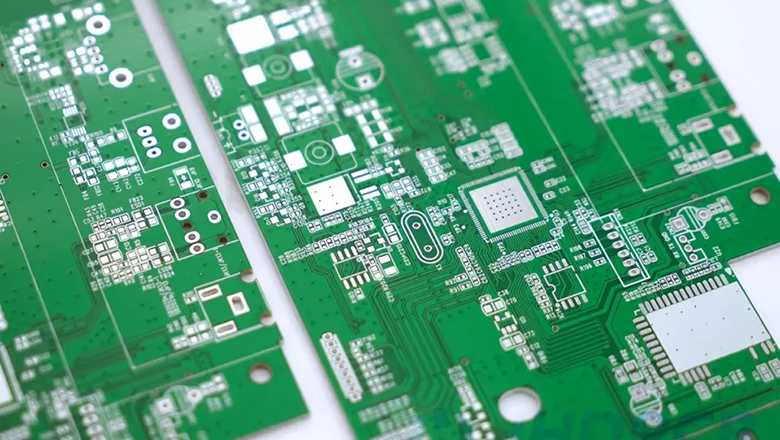
There are many names we often hear, such as “solder mask layer”, “solder mask ink”, or simply “green oil”. It is merely that layer of colored coating covering almost all PCB surfaces. It is a crucial step in the entire PCB manufacturing process that provides the originally exposed copper foil circuits with a permanent “protective armor”, enabling them to enter the mass production stage. It not only blocks the moisture in the air to prevent oxidation, but also physically isolates the risk, preventing short circuits caused by the accidental connection of those fine copper wires.
This is a layer of “armor” formed by polymer resin or epoxy resin. Through precise coating and exposure developing processes, we make it “open the window” only in one place – all areas except for the pads, through holes and connectors that need to be welded or conductive will be tightly covered by this oil film.
Where Do You Find the Solder Mask Layer?
You’ll see solder masks as the green, blue, black, red, or even clear overlays spanning most of a PCB’s visible surface—except for shiny exposed pads and via holes. The mask is an essential process for both surface-mount technology (SMT) and through-hole assembly, preserving the integrity of each copper trace.
Functions of Solder Masks
The functions of solder masks are far-reaching and vital to high-yield, robust PCB manufacturing and assembly:
- Oxidation and Corrosion Protection:
This is actually the most fundamental task of the solder mask layer. The bare copper foil on the PCB is vulnerable to erosion by air and moisture. Applying a solder mask is equivalent to putting a “raincoat” on the circuit, preventing oxidation and blackening.
- Prevention of Short Circuits:
In the process of doing design or maintenance. If the pad spacing on the board is very small and there is no solder mask to block it, once the reflow soldering passes, the molten solder paste can easily bridge and connect together. Protect the welding range by using a solder mask layer.
- Mechanical and Chemical Defense:
There are many processes on the PCBA production line, such as flux passing, cleaning, and being easily scratched by mechanical arms. The solder mask prevents erosion by chemical agents and minor physical scratches.
- Aesthetic Appeal and Inspection:
The solder mask is available in various colors, including green, blue, red and black. However, from the perspective of our production end, green remains the mainstream – because it reflects the softest light under AOI optical inspection, is easy for operators to distinguish, and has high screen printing recognition.
- Moisture and Dust Protection:
The PCBA covered by the casing is not sealed. Changes in temperature and humidity during daily use and dust accumulation may cause the performance of components to drift. The solder mask seals the entire board surface, making the board naturally more durable and having a longer lifespan.
Types of Solder Masks
1. Epoxy Liquid Solder Mask
- Applied with silkscreen printing; quick and cost-effective for prototypes and low-density boards.
- Not ideal for very fine-pitch components due to limited resolution.
2. Liquid Photoimageable Solder Mask (LPSM, LPI)
- The most widely used in the PCB industry for its fine feature definition and compatibility with dense assemblies.
- Sprayed or curtain-coated onto the PCB, then patterned by UV exposure using a photomask or direct laser imaging.
- Especially suited for modern HDI or high-density interconnect.
3. Dry Film Photoimageable Solder Mask (DFSM)
- Laminated as a solid film, then imaged and developed.
- Offers extreme precision, so it’s favored for advanced applications like BGA, CSP, or medical-grade boards.
Solder Mask Types
| Solder Mask Type | Application Method | Best For | Pros | Cons |
| Epoxy Liquid | Silkscreen Printing | Prototypes, simple boards | Inexpensive, fast | Less precise, lower yield |
| LPI | UV Exposure | Fine-pitch, dense, advanced PCBs | High accuracy, reliable | Requires cleanroom process |
| DFSM | Dry Film Lamination | Ultra-fine/high-cost boards | Superior definition, robust ink | More costly, complex |
Solder Mask Materials and Application Process
Quality begins with materials. PCB manufacturers use epoxy, LPI, or DFSM solder mask ink—all engineered to resist high soldering temperatures, aggressive cleaning, and environmental challenges.
Application of Solder Mask
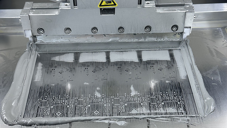
- Surface Cleaning: Vital to remove all contamination, ensuring that mask and solder bonds to copper securely.
- Coating: Apply the solder mask ink evenly over the board surface. The method is as follows: Use screen printing for regular boards; High-precision boards are coated by spraying or curtain coating. The thickness is usually controlled between 20 and 50 microns. It’s too thin and the ink is prone to cracking. It’s too thick. The ink flows to the edge of the pad.
- Imaging: The board that has been coated with ink will next pass through the exposure machine. First, cover the board with a film (or directly scan it with a laser), allowing ultraviolet rays to pass through the film and shine on the ink. The ink exposed to light will undergo a polymerization reaction. For high-precision circuits, we use LDI (Laser Direct Imaging) technology, which is suitable for HDI boards with particularly small pads and dense spacings.
- Developing: After exposure, the board was pushed into the developer. The ink that was not exposed to ultraviolet light was quickly washed away, and the copper foil on the solder pads and test points was thus exposed spotlessly. The “window” on the board was thus formed.
- Curing: The ink that has been developed has not yet fully “set” and needs to be put back into the oven or a strong ultraviolet curing oven for baking. This step is to ensure that the ink hardens thoroughly, achieving sufficient hardness and adhesion.
- Inspection: Visual and AOI ensure coverage, color, and dam width between pads meet spec.
What is a Paste Mask?
Paste mask and paste masks refer to a digital layer in your PCB design—not a physical layer on the finished board, but every bit as important. The paste mask layer defines locations where solder paste is to be applied onto the PCB during SMT assembly.
Paste mask is also called the “cream” or “stencil” layer. It is essential because it forms the basis for creating the physical stencil—a precisely laser-cut piece of stainless steel or polyimide film—used to apply solder paste onto solder pads for SMD components in PCB assembly.
- The paste mask is a temporary mask: The steel mesh layer, also known in the industry as the “solder paste layer” or “steel mesh”. Its most distinctive feature is that it is not left on the board.
Its mission is very pure – at the moment of printing solder paste, it acts as a precise “mold”. Holes are drilled on the steel mesh according to the position of each solder pad and covered on the board. The scraper pushes the solder paste once, and the solder paste passes through these small holes, falling precisely and accurately onto each SMD solder pad. The steel mesh layer is the “guiding star” in the SMT process. The solder paste applied to the pads is determined by the opening size and thickness of the mesh. If too much solder paste is given, the reflow soldering is prone to short circuits. If the amount was insufficient, false welding and setting up steles all followed suit.
Functions of Paste Masks
The primary purpose of paste masks in PCB manufacturing and assembly is to guarantee that solder paste is accurately placed just where it’s needed. The paste mask is essential for:
- Defining Solder Paste Deposition: Based on the steel mesh layer data in the design documents, the positions of the apertures (openings) on the steel mesh are directly determined. These openings precisely correspond to each component pad on the board that requires soldering.
- Ensuring Solder Volume Consistency: The strength and reliability of solder joints largely depend on the amount of solder paste. The shape, size and thickness of the holes in the steel mesh determine the volume of solder paste printed each time. Especially when dealing with high-density, fine-pitch devices like 01005 and 0.4mm pitch QFN, LHD TECH engineers will repeatedly deliberate during the steel mesh design stage – whether this mesh can fill every pad depends entirely on data.
- Speeding Up the Assembly Process: Manual solder paste application is limited to sample quantities. Bulk orders rely on the “precise replication” of steel mesh. The automatic printing machine can brush over ten or twenty boards per minute, and the amount and position of solder paste on each board are almost exactly the same. This repeatability of precision is precisely the capability that the steel mesh layer endows the production line with.
- Preventing Manufacturing Errors: Many welding defects can easily be found in the design of steel mesh. If the hole opening is off, the solder paste will be printed crooked. If the opening is too small, there will be a lack of tin at the bottom of the component. Therefore, in the DFM (Manufacturability Analysis) stage before production starts, we will strictly review the alignment accuracy of the steel mesh layer – to ensure quality.
Types of Paste Masks and Stencils
While the concept of a paste mask remains the same, there are several stencil strategies to support different PCB designs:
- Top and Bottom Paste Masks: Most modern PCBs have top and bottom paste mask layers, allowing for double-sided assembly. Top and bottom paste masks ensure you have precise solder paste control whether components are placed on one side or both. These are essential for high-density and multifunction PCBs.
- Step Stencils and Multi-level Stencils: Stepped steel mesh is a type of steel mesh with more than two thicknesses. The steel mesh in the large pad area is partially thickened. The thin-pitch pins are afraid that the pads at the short-circuit point will be locally thinned. A net is set up in different thicknesses, allowing everyone to take what they need. For instance, the power board and the main control board are produced together, while the power tubes and the CPU each have their own tin content to ensure no problems occur after passing through the furnace.
- Prototype vs. Production Stencils:
- Prototype stage: Choose hand-attached or semi-automatic patching. Using Mylar polyester film steel mesh can ensure product quality, and it has low cost and short delivery time.
- Mass production stage: It is necessary to ensure stable and accurate quality. LHD TECH uses laser-cut stainless steel mesh throughout its entire line, with precision controlled at the micrometer level. A good steel mesh, after being printed hundreds of thousands of times, still has sharp edges of the holes, does not stick to tin, and does not deform – this is the basic basis of yield.
Paste Mask Application Process
Here’s how the paste mask works through the pcb manufacturing and assembly sequence:
- Paste Mask Layer Definition: The designer defines the paste mask layer in CAD. Openings on paste mask represent all pads that will receive solder paste.
- Gerber Export: After the design is finalized, our engineers will separately export the Paste Mask layer from the PCB design file, which is commonly known as the “steel mesh layer” or “solder paste layer”. The Gerber files exported from this layer will be directly sent to the steel mesh manufacturer.
- Stencil Fabrication: After receiving the documents, the steel mesh factory will use a high-power laser to precisely cut openings on the stainless steel sheets according to the position, shape and size of each pad in the Gerber. The precision of this step is required to be controlled within ±5 microns – a slight deviation could cause the subsequent patches to be crooked.
- Stencil Printing: After the steel mesh is delivered to the production line, the first thing to do on the machine is to align it. The operator will fix the steel mesh on the printing machine. The board is fed in from the track, the top pin lifts it up, and the steel mesh drops, tightly adhering to the board surface. Then the scraper pushed the solder paste once – the solder paste was squeezed into every opening of the steel mesh and precisely landed on the pads below.
- Stencil Removal: After the printing is completed, the steel mesh needs to be slowly and smoothly “detached” from the board. The professional term for this is “demolding speed”. In our process parameters, both the speed and distance of this step have been repeatedly verified.
- SMT Placement and Reflow: The steel mesh was taken away, and now each pad on the board was topped with a small, neatly arranged lump of solder paste. Next, the surface mount technology (SMT) machine comes on stage. The suction nozzle picks up the capacitors, resistors, and chips, and the vision system aligns the positions. The board with the components attached enters the reflow oven and goes through four temperature zones: preheating, constant temperature, reflow and cooling. The tin powder in the solder paste melts and then solidifies, firmly bonding the component pins and pads together.
Solder Mask vs Paste Mask: Key Differences and Functions
| Aspect | Solder Mask Layer | Paste Mask Layer |
| Function | PCB protection, insulation, and solder area definition | Defines precise solder paste application |
| Type | Permanent layer applied during pcb manufacturing | Temporary stencil used during PCB assembly |
| Material | Epoxy/LPI/DFSM solder mask ink and polymers | Laser-cut stainless steel or mylar (for stencil) |
| Color | Green, red, blue, black, white, and more | Stencils are metallic/gray; digital layer colorless |
| Use Stage | During PCB manufacturing | During PCB assembly |
| Openings/Exposure | Openings expose copper pads/vias for soldering | Openings match SMD pads for paste application |
| Error Risk | Wrong mask: shorts/oxidation | Wrong mask: poor or excess solder, misplacement |
| Lifetime | Solder mask is a permanent protective shield | Paste mask is a temporary stencil |
Quick Summary
- Solder mask is used in the pcb manufacturing process: it runs through the entire PCB manufacturing process and is a permanent physical barrier. Its responsibility is very clear: to tightly protect the copper foil, isolating it from air and moisture. Precisely define the window area for each pad; At the same time, during soldering, firmly block the molten solder to prevent bridging and short circuits between adjacent solder joints.
- Paste mask is essential: It only appears in the SMT assembly stage and is the absolute “protagonist”. Its task is to guide the solder paste to fall onto the pads precisely in volume and position through the openings on the steel mesh. Ensuring welding quality, production efficiency and process consistency will all get out of control.
Mask Layers in PCB Design Files
Design tools export both solder mask and paste mask layers for manufacturing precision:
- The solder mask layer defines areas with no solder mask (pads/vias), ensuring correct copper exposure.
- The paste mask layer defines where solder paste is to be applied—matching all SMD pads intended for soldering.
How Solder Masks and Paste Masks Work Together
The interplay of masks and paste masks is crucial for zero-defect pcb manufacturing and assembly:
- The pcb solder mask protects all copper except for necessary solder pads. It creates a durable, insulated surface.
- The pcb paste mask guides the application of solder paste right on the open pads, supported by the solder mask openings. The combination ensures only the correct amount of solder is applied, reducing excess solder, bridging, or weak connections.
Essentially, using the right mask and solder paste process is not optional—it’s the backbone of high-performance, reliable printed circuit board products.
Applications and Uses in the PCB Industry
Mask and solder paste technologies empower modern PCB designs from every vertical:
- Consumer Electronics: The boards in mobile phones and watches are packaged in BGA and CSP, with very tight pad spacing. In this scenario, strictly control the opening accuracy of the steel mesh layer to prevent problems such as short circuits and false welding.
- Automotive & Aerospace: Automotive-grade and aerospace-grade boards cannot be replaced easily. The temperature difference between -40℃ and 150℃ in the engine compartment, prolonged vibration, and erosion by salt spray and moisture – all these impose extremely high requirements on the solder mask layer. When selecting materials, the heat resistance, adhesion and insulation resistance of solder mask ink are all hard indicators.
- Medical Devices: After the medical equipment is repeated hundreds of times, the board must not have any performance drift. When manufacturing this type of board, the compactness of the solder mask layer, the absence of voids and micro-cracks are key points to be controlled. The steel mesh layer must ensure that the IMC (intermetallic Compound) layer at each weld point is uniform and dense.
- Wearables and IoT: Ultra-miniature boards rely on minimal but precise solder mask and paste mask features for both aesthetics and maximum component density.
Common Defects and Solutions: Mask and Solder Paste
| Defect/Problem | Common Cause | Solution / Prevention |
| Solder Bridges | Insufficient mask dam width, excess paste | Increase mask barrier, refine stencil |
| Voids/Misalignment | Poor mask registration, mask shrinkage | AOI checks, strict fab tolerance |
| Cold/Poor Solder Joints | Insufficient solder paste, aperture clogged | Clean/replace stencil, adjust paste |
| Solder Balling | Excess solder paste, stencil too thick | Reduce aperture, thinner stencil |
| Corrosion Under Mask | Mask material defect, poor curing | Use qualified ink, verify process |
Essential Design Tips for PCB Solder Mask and Paste Mask
- Keep mask expansion tight: Openings on solder mask layer should be only slightly larger than the copper pads, just enough to account for fab registration tolerance.
- Paste mask apertures must match—or slightly reduce compared to—the underlying pad: When determining the opening size of the steel mesh, it is required to be the same size as the solder pad or slightly smaller than it. After passing through the furnace, the solder paste will melt, collapse and spread, flowing onto the solder mask layer and forming a bridge. A slightly smaller “dam” that can rely on the solder mask layer.
- Choose compatible materials: The board needs to pass through 260℃ reflow soldering, so the ink must be able to withstand high temperatures. The boards are used in chemical plants, so the ink must be resistant to corrosion. The board is used outdoors, so the ink must be able to shield against ultraviolet rays and moisture. The mismatch of materials will be full of hidden dangers in the later stage.
- Maintain clear design documentation for every mask and solder operation: The details such as the size of the window for the solder mask layer, the type of hole for the steel mesh layer, and which area needs to be stepped treatment were described very clearly during the design stage. Our internal standard is: Drawings are contracts and documents are evidence.
Frequently Asked Questions
What is the difference between solder mask and paste mask?
- Solder Mask:It is a permanent protective coating applied during the PCB manufacturing process. Its purpose is to wrap the copper foil of the circuit to prevent oxidation and short circuits, and at the same time precisely inform the subsequent processes by “opening the window”.
- Paste Mask:It is not something left on the board, but a design document and the steel mesh made based on this document. It only appears in the SMT assembly stage, and its task is to guide the solder paste to fall onto the pads precisely in volume and position through the openings on the steel mesh.
What happens if paste mask apertures are misaligned?
On the pcb manufacturing and assembly process. line, we have a repeatedly emphasized bottom line: the openings of the steel mesh layer must be precisely aligned with paste mask apertures, and the steel mesh printing is a zero-tolerance process. For instance, operational deviations can easily lead to: the solder joints being directly scrapped; Components are misaligned or even tombstones are erected. Short circuit and plate burning; Cold welding and false welding; The most extreme case is the lack of functionality.
So before each new steel net machine, it must pass through two “security checks” :
- Alignment calibration: Use optical alignment tools to confirm that the overlap between the steel mesh opening and the solder pads on the plate is within the tolerance range.
- First piece verification: After printing the first board, pass it through the furnace, place the surface mount, and conduct an inspection. Only when all solder joints are confirmed to be normal can the operation continue.
Is it possible to modify or repair a solder mask or paste mask layer after manufacturing?
- We often say: “If the solder mask goes wrong, it usually means a major operation is needed.” There’s a problem with the steel mesh layer. Just change the mold and it’s done.”
- If it’s just a minor problem with the solder mask ink, such as a scratch caused during the production process or a pinhead-sized hole left during exposure and development, we can repair it locally by applying ink.If there are large-scale problems, such as the window opening position being off, the ink thickness being uneven, or even the entire piece peeling off, the board can only be reworked or even redone.
- Problems with the paste mask layer – such as incorrect opening dimensions or misaligned positions – can be resolved simply by remaking a new steel mesh.
How do I ensure I have used the right solder mask and paste mask layers in my Gerber files?
Double-check in your PCB CAD tool and in a Gerber viewer. The solder mask layer is one part on the PCB that shows openings only where pads/vias should be exposed. The paste mask layer (often called “cream” layer) should match all surface mount pads where solder paste is to be applied onto the pcb. If there is ever confusion, consult your pcb manufacturers or assembly house for a design review prior to release.
Does every PCB need both solder and paste masks?
Most professional pcb manufacturing for modern electronics will require both a solder mask (to protect copper and define pad openings) and a paste mask (for stencil-based deposition of solder paste during assembly). In rare cases, such as heavy-duty power boards or certain experimental prototyping, one or the other may be omitted—but this is almost never advisable for any mass production or precision work.
Expert Best Practices: PCB Manufacturing and Assembly
- Always run a DFM check: Before sending files to fabricators, employ automated design rule checks on both your solder mask and paste mask layers. This catches possible shorts, insufficient solder, misalignments, or design rule violations.
- Minimize openings on the solder mask for maximum protection: Allow only as much exposure as necessary for soldering process or test access.
- Match stencil thickness to your smallest aperture: Thinner stencils are essential for fine-pitch, high-density layouts, while thicker stencils may be used for larger power components. Consult with your assembly shop regarding the ideal thickness and stencil technology.
- Inspect the first assembled units: Use SPI (Solder Paste Inspection) and AOI to validate solder mask coverage, stencil registration, and overall assembly quality. Address any defects immediately before mass build.
- Document mask and solder process choices: Keep revision-controlled records specifying every mask ink, stencil type, and relevant settings. This aids troubleshooting, quality improvement, and repeatability for future projects.
Conclusion: Choosing and Optimizing Mask Layers for High-Quality PCBs

In the world of pcb manufacturing and assembly, mastering the differences and functions of the solder mask vs paste mask can mean the difference between field failures and five-star product reliability. The solder mask is a permanent, vital shield over your circuitry—preserving copper, preventing shorts, and creating a robust platform for every pcb assembly run. The paste mask (realized in the physical form of a stencil) is a temporary, but essential, template that ensures only the precise amount of solder paste lands on the correct pads, supporting flawless, repeatable assembly outcomes.
Getting the application of solder mask and application of solder paste right requires attention to materials, process, alignment, specific product needs, and close collaboration with your pcb manufacturers and assemblers. As the PCB industry moves to finer pitches, tighter footprints, and ever-higher reliability requirements, these mask layers are more crucial than ever—not just for manufacturability, but for end-user safety and satisfaction.
Call to Action
Are you experiencing challenges with mask and solder paste in your current project? Need advice on pcb manufacturing choices, or do you want a detailed DFM review before your next production run?
Contact us for expert support— or subscribe to our newsletter to access the latest in mask technology, stencil design, and pcb manufacturing and assembly innovations. Share your experiences, ask questions below, and let’s build the most reliable boards together.