Introduction
The electronics manufacturing industry is currently in a phase of rapid development. This sector places extremely high demands on the assembly quality of printed circuit boards. Modern printed circuit boards have reached an unprecedented level of complexity. The structural design of these boards is very compact. Their functional importance is also increasingly prominent. The mounting density of electronic components is continuously increasing. The geometric dimensions of solder joints are constantly shrinking. Against this technological backdrop, traditional inspection methods reveal their limitations. These methods struggle to effectively identify hidden defects. They also struggle to effectively identify internal defects.
Automated X-ray inspection technology currently holds a significant position in the PCB manufacturing industry. This technology is widely applied in the fields of quality control and high-end inspection. The inspection system utilizes advanced X-ray technology. The system is also equipped with sophisticated image analysis algorithms. This combination enables deep-level, non-destructive testing. The system can accurately identify a variety of hidden defects. Defects such as voids, solder bridges, component misalignment and internal cracks can be detected. These defects are often difficult to find using other inspection methods.
This comprehensive guide systematically elaborates on the core principles, practical applications and key advantages of X-ray inspection in PCB assembly.It highlights the indispensable role of this technology in modern electronic product manufacturing, with a wide range of application scenarios covering consumer electronic devices as well as aerospace and medical devices demanding high reliability.
Understanding X-Ray Inspection in PCB Assembly
What Is X-Ray Inspection?
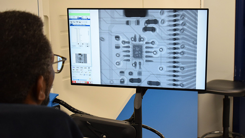
X-ray inspection is a technical method that utilizes X-ray radiation for detection purposes. This technology is primarily used to observe the internal structural features of PCB assemblies. Basic inspection methods, such as visual inspection, can only obtain information from the product’s surface. In contrast, an X-ray inspection system is capable of revealing the internal conditions of a PCB. This imaging technology can expose the internal structural states of complex PCBs that are not visible from the outside.
- The implementation of X-ray inspection typically relies on modern X-ray equipment. Such equipment is equipped with a high-performance X-ray tube. The system also integrates advanced detectors and analysis software. These components work together to perform the inspection task.
- An X-ray beam can pass through the object under inspection. A fully assembled PCB board is a common subject of such inspection. Density varies across different areas within the object. The X-ray beam exhibits varying penetration effects based on these density differences. The inspection equipment utilizes these penetration effects to clearly reveal hidden solder joints, as well as voids and various other defects.
Principles and Importance
The underlying principles of automated X-ray inspection are similar in some ways to automated optical inspection (AOI)—they both compare actual assemblies to known “good” reference images. However, AOI relies on visible light and can’t see through components, while X-ray inspection uses high-resolution X-ray radiation for internal assessment.
X-Ray inspection in PCB assembly has become a key enabler for:
- Detecting hidden defects in high-density, complex PCB assemblies.
- Ensuring quality in grid array packages like BGA (ball grid array) and QFN/LGA.
- Advanced inspection coverage for both SMT and through-hole components.
With the ongoing evolution of X-ray inspection technology, electronics manufacturing now delivers unprecedented reliability in modern electronic assemblies.
How X-Ray Inspection Works
Understanding X-ray inspection in PCB assembly starts with the basics:
The X-Ray Inspection Process
1. X-Ray Tube and Beam: The X-ray tube generates controlled X-rays. The beam is directed toward the PCB assembly. This beam is capable of penetrating all components and solder joints.
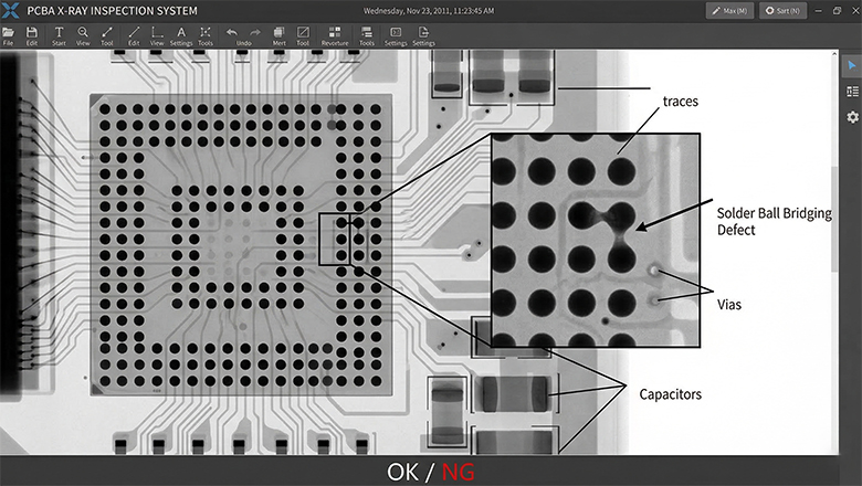
2. Object Under Inspection: There is a difference in the ability to absorb X-rays between high-density materials and low-density substrates. High-density materials such as solder balls, copper traces and leads can absorb a greater amount of X-ray energy. Lower-density substrate materials, on the other hand, absorb less X-ray energy. These differences in absorption are ultimately translated into contrast in the inspection image.
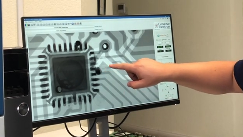
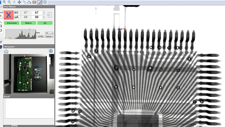
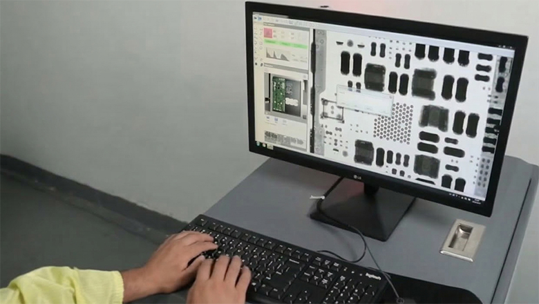
3. High-Resolution Detectors: X-ray inspection equipment operates using digital flat-panel detectors. The equipment can also employ linear sensors to capture X-ray signals. These detectors are responsible for receiving the X-ray beam, which has undergone intensity variations. The system subsequently processes the received signals. The final generated digital image possesses a dual-presentation capability. This image can display the surface condition of the PCB. It can also simultaneously reveal its internal structural features.
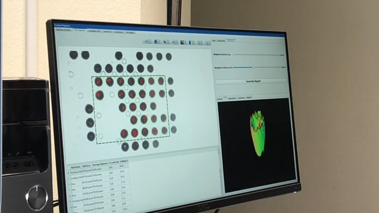
4. Advanced Inspection Software: Automated X-ray inspection systems rely on software to perform analysis. This software integrates a variety of complex algorithms. These algorithms perform computational analysis on the images captured by the system. The software is capable of independently completing recognition tasks. It can detect and classify various types of assembly issues. These issues include defects such as hidden voids, solder bridges, and component misalignment, all of which can be identified. The software can also measure the specific values of these defects.
5. Inspection Results: The system is capable of identifying PCB boards with defects. The system performs a marking process on these defective boards. The system also generates a detailed inspection report. This report can be used for quality tracking work, process control and compliance review processes.
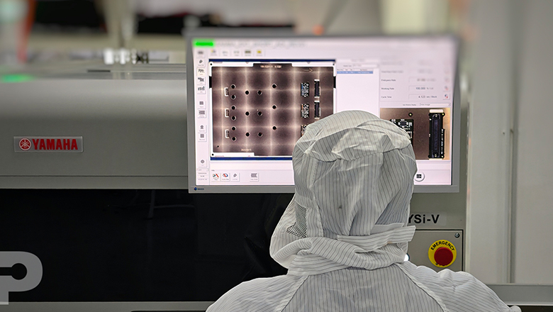
Modern X-ray inspection systems also allow for both inline X-ray inspection (real-time, on the assembly line) and batch inspection for prototypes or failure analysis.
Types of X-Ray Inspection Systems in PCB Manufacturing
2D X-Ray Inspection Systems
A 2D X-ray inspection system performs scanning from a fixed angle. The system captures shadow images from this angle. These images are used to quickly assess solder joint quality. The system observes the general internal structural features of the PCB through the images.
- Strengths: Fast, suited for inline inspection, suitable for surface-mount and through-hole assemblies.
- Limitations: May miss defects obscured by overlapping structures.
3D X-Ray Inspection Systems and Computed Tomography (CT)
- 3D/CT X-ray systems: Construct a multi-layered, volumetric image using rotation and multiple angles. This enables virtual slicing and inspection depth analysis, essential for uncovering hidden defects within complex PCB structures.
- Ideal for: BGAs, advanced grid array packages, and assemblies requiring inspection of all sides of the PCB.
Tomosynthesis and Advanced Inspection Systems
- Tomosynthesis: Produces quasi-3D stacked images, balancing speed and depth.
- Advanced systems: AI technology has been integrated into the inspection system. This system is capable of operating in dense electronics manufacturing environments. The system has achieved automatic defect recognition functionality. Inspection coverage has also been enhanced through this technology.
| X-Ray System | Inspection Depth | Application | Strength |
| 2D AXI | Surface to mid | SMT, THT | Speed, efficiency |
| 3D CT | Full volumetric | BGA, QFN, HDI | Inspection coverage, depth detail |
| Tomosynthesis | Layered | Dense PCBs | Quick pseudo-3D, affordable |
What Defects Can X-Ray Inspection Systems Detect?
Automated X-ray inspection in PCB assembly is the only electronics manufacturing technology that consistently reveals certain classes of critical internal defects:
Solder Joint Defects
- Solder Voids/Porosity: X-rays can penetrate materials and reveal their internal structures. Inspectors utilize this property to observe the interior of BGA balls. They also use it to check for the presence of voids inside solder joints. X-ray inspection is one of the few technical methods capable of performing such detection. The presence of voids can weaken the mechanical strength of a solder joint. Voids can also affect the reliability of the electrical connection. Both of these effects manifest as a significant decline in performance.
- Solder Bridging/Shorts: X-ray inspection technology possesses specific detection capabilities. This technology can identify solder bridges present beneath grid arrays. It can also detect solder splashes occurring underneath connectors. These defects are typically hidden from view.
- Insufficient Solder/Open Joints: AXI systems can detect incomplete wetting or open joints where electrical connectivity is at risk.
Component and Placement Defects
- Misaligned Components: Three-dimensional inspection systems and two-dimensional inspection systems possess specific recognition capabilities. These systems can detect tombstoned components, shifted components, or tilted components. Automated optical inspection technology struggles to identify the aforementioned component defects. Manual visual inspection also finds it difficult to detect these issues. The inspection systems function by identifying these defects. The quality of component placement is thereby improved overall.
- Head-in-Pillow (HIP) and Cracks: Especially in BGA inspection, X-ray machines expose HIP defects, micro-cracks and even internal delamination—ensuring quality of solder joints in modern PCB assemblies.
Internal and Structural Defects
- Pin-through-hole (PTH) Fill: Inspection coverage extends to PTH barrels, measuring solder fill percentage per IPC-A-610 standards.
- Delamination and Layer Voids: Using X-ray, engineers can see internal PCB layer separation, moisture pockets and foreign object inclusions.
Key Applications for Automated X-Ray Inspection in PCB Assemblies
Automated X-ray inspection isn’t just a tool—it’s an essential pillar of advanced inspection in modern electronics manufacturing. Here’s where AXI plays a vital role:
Process Control and Inline Inspection
- The inline X-ray inspection system operates continuously on the production line. This system provides real-time feedback information during the production process. The inspection system scans the circuit boards before they enter downstream processes. The system is capable of identifying soldering issues and assembly defects. These problems are flagged before proceeding to subsequent stages.
- Real-time inspection results allow for process adjustments, such as reflow oven tuning or stencil replacement, optimizing both speed and assembly quality.
Prototyping and PCB Development
- During the product development stage, prototype PCB boards are subject to various causes of issues. At this stage, the design scheme for the PCB prototype is not yet fully mature. The development team may adopt new types of electronic components that have not been fully validated. Assembly processes are also frequently subject to changes and adjustments. These factors make the prototype boards prone to internal hidden defects. X-ray inspection systems provide rapid feedback on these prototype boards. The development team uses this feedback information to adjust the design scheme in a timely manner. Early design improvements can thus be implemented during the development phase. This approach effectively reduces costly, repeated iterations. The final quality and reliability of the electronic product are consequently enhanced.
Final Quality Inspection and Audit
- For sectors such as medical, automotive, and aerospace electronic manufacturing, automatic X-ray inspection is the last checkpoint before shipment. The ability to ensure quality by confirming that all solder joints—including hidden solder joints and PTH barrels—are free from internal defects gives OEMs and EMS companies confidence in their shipment.
Regulatory Compliance and Documentation
- AXI is indispensable in producing mandatory quality control documentation for certificates of conformance, automotive PPAPs or medical device DHRs. Inspection results are stored, archived, and made available for regulatory audits as part of comprehensive PCB inspection standards.
Benefits of X-Ray Inspection: Why Modern PCB Manufacturing Relies on It
Let’s highlight the many benefits of X-ray inspection that make it a cornerstone in today’s electronics manufacturing:
1. Superior Detection of Hidden Defects
- X-ray inspection reveals hidden defects that AOI, ICT, and functional tests cannot find, including voids, bridges and internal cracks deeply embedded in multilayer PCB structures.
- Systems can detect hidden solder joints, BGA grid array failures, PTH fill percentages, and even layer delamination, thus ensuring unmatched assembly quality.
2. Non-Destructive Testing (NDT)
Unlike destructive cross-sectioning, X-ray inspection is a truly non-destructive testing method. Automatic X-ray inspection maintains board integrity, allowing electronics manufacturers to test every assembly without scrap or waste.
3. Process Optimization
By leveraging collected inspection data, manufacturers can correlate defect trends with process variables—making X-ray inspection a continuous improvement tool for solder joint quality, pick-and-place calibration and solder paste application.
4. Inspection Coverage and Versatility
AXI expands inspection coverage well beyond surface-level AOI, making it the preferred advanced inspection technology for complex PCB designs.
5. Enabling the Most Reliable Electronic Products
Whether for mission-critical aerospace flight controllers, implantable medical devices or automotive ECUs, AXI helps ensure that only high-quality, defect-free boards reach the customer.
X-Ray Inspection vs AOI and Visual Inspection
| Inspection Method | What It Sees | Best For | Weaknesses |
| Visual Inspection | Surface only | Prototypes, simple PCBs | Misses hidden/internal defects |
| AOI | Surface, silkscreen, paste | SMT, mass volume | Can’t see through or beneath parts |
| Automated X-Ray | Internal and external features | BGAs, QFNs, PTH, dense/complex PCB assembly | Higher cost, slower than AOI |
| In-Circuit Test | Electrical connectivity | Final test, simple faults | No physical or assembly insight |
Best Practices for Implementing Automated X-Ray Inspection
1. Assess High-Risk Areas First
Start by mapping out which areas of your assembly have the greatest risk of hidden defects (BGAs, PTHs, stacked components), and focus X-ray inspection resources there.
2. Calibrate Regularly
Regular calibration of X-ray machines and software thresholds ensures the fidelity of inspection results and reduces both false positives and negatives.
3. Integrate With MES/ERP
Connect your inspection process to your Manufacturing Execution System for batch traceability and real-time process analytics.
4. Combine AOI and AXI
Leverage both AOI and AXI. AOI provides speed for visual inspection of surface features, while AXI delivers depth for detecting hidden defects.
5. Train Your Team
Ensure operators and quality engineers understand not just how X-ray systems work, but also how to interpret subtle internal defect signatures.
6. Use Inspection Data for Continuous Improvement
Track defect trends by lot, time, placement machine, and supplier. Use this advanced inspection data to continually refine your PCB manufacturing process.
Technical Considerations and Limitations
While modern X-ray inspection vastly improves inspection coverage, several technical factors affect its performance:
Resolution and Inspection Depth
- Higher-resolution X-ray machines are needed for fine-pitch and microvia applications. However, increasing resolution can slow throughput, so a balance should be maintained.
X-Ray Radiation Safety
- Today’s x-ray inspection systems are heavily shielded and adhere to strict radiation safety protocols, but operators must still be trained and systems must comply with all local regulations.
Cost vs. Benefit
- 2D inspection is less costly but might miss internal defects in highly complex PCB assemblies. 3D and CT can be expensive; however, for advanced electronic assemblies, they are often essential for true quality control.
Image Analysis and AI
- Interpreting complex images and distinguishing between critical and non-critical defects (e.g. acceptable void percentages) may require experienced personnel and advanced AI inspection software.
Industrial Standards and Regulatory Compliance
X-ray inspection in PCB assembly is often required to meet:
- IPC-A-610: Solder joint acceptability, barrel fill and void percentage standards for PCB quality.
- IPC-7095: Guidance for BGA inspection and ball grid array assembly quality.
- J-STD-001: Soldered electrical and electronic assemblies workmanship and quality inspection.
- ISO 13485: For medical device reliability, demanding measurable, documented advanced inspection coverage.
Future Trends: The Evolution of X-Ray Inspection Technology
The evolution of X-ray inspection technology is pushing the boundaries of what’s possible in modern PCB manufacturing:
AI-Powered Inspection and Big Data
- Machine learning is making advanced inspection systems smarter, speeding up automated classification and adapting to new assembly issues in real time.
Real-Time 3D (CT) X-Ray Inspection
- True volumetric inspection that slices through a circuit in real-time is becoming a reality—even at production line speeds. This drastically increases the ability to reveal hidden defects.
Cloud Connectivity
- Inspection results and X-ray images are increasingly networked for global accessibility, Supplier audits, and instant customer reporting—supporting both manufacturing quality control and regulatory compliance.
Sustainability and Miniaturization
- New X-ray machines use lower X-ray radiation doses, faster scanning, and smaller footprints for deployment in miniaturized smart factory lines.
Predictive Quality
- Integrating inline X-ray inspection data into digital twin simulation allows manufacturers to predict reliability and enable process optimization for each unique PCB.
FAQs: X-Ray Inspection in PCB Assembly
Q: Why is X-ray inspection essential in modern electronics manufacturing?
A: X-ray inspection reveals hidden and internal defects, ensures solder joint integrity, and provides unmatched quality control for densely populated and complex PCB assemblies.
Q: Which components require X-ray inspection most urgently?
A: BGAs, grid array devices, QFNs, LGAs and fine-pitch SMT components—all rely on AXI to detect internal defects that surface inspection methods miss.
Q: Is automated X-ray inspection safe for electronic assemblies and operators?
A: Yes. All modern X-ray inspection systems rigorously control X-ray radiation and are engineered for safe, non-destructive inspection.
Q: How does X-ray inspection compare to AOI?
A: AOI is ideal for surface and markup inspection. X-ray inspection is required for hidden solder joints, PTH fill, detecting internal defects and advanced inspection coverage.
Q: Can X-ray inspection results be used for regulatory and customer audits?
A: Yes. Automated X-ray inspection generates traceable, archivable data that demonstrates robust inspection process and ensures compliance with strict industry standards.
Conclusion
The evolution of X-ray inspection technology continues to redefine what’s possible in PCB manufacturing and electronic assembly quality. Automated X-ray inspection is no longer optional in the world of modern, miniaturized and mission-critical electronic assemblies. For every board, every solder joint, and every shipped device, X-ray inspection remains the cornerstone of advanced inspection, quality assurance, and a proactive approach to defect prevention.
By embracing both automated X-ray inspection and AOI, manufacturers set a new benchmark in defect detection, process control, and long-term product reliability—ensuring the future of electronics is safe, robust, and trusted, one invisible solder joint at a time.