What is PCB First Article Inspection?

In PCB production and assembly, First Article Inspection (FAI) is a standardized and traceable quality control process that we must implement. Its main purpose is to verify that the first prototype of a new or revised design fully complies with every requirement of the engineering drawings, layout design, and BOM (Bill of Materials). Unlike simple dimensional verity, our FAI covers both physical characteristics and electrical functions: from mechanical parameters, such as board thickness, hole diameter, and trace width and spacing, functional indicators such as conductivity and insulation performance, ensuring every detail aligns with design specifications and avoiding systemic deviations during mass production.
Defining FAI in Electronics Manufacturing
For the PCB field, FAI (Feature Inspection and Testing) is typically arranged after prototype verification and before mass production—an important point is to control mass production risks. It’s not just a single test, but a complete quality step:
- Checkthe PCB design of the first board one by one: include pcb size, hole size, tolerances, copper thickness, to ensure all aspects are matching with customer’s Gerber files.
- Carefully checkthe PCBA soldering and component position to avoid assemble mistakes, such as wrong components, or solder joints.
- Confirm allthe materials and specifications and components meet the customer’s requirements, cut the material usage mistake from the source.
- Using a very strict quality inspection standard to ensure every process is 200% perfect, to keep the stability and best quality.
The most importantly, FAI is not only a verification of the PCB design itself, but also a check on our capabilities across the whole process from solder paste printing and reflow soldering to final functional testing. It helps customers mitigate quality risks in the mass production stage and ensure product reliability.
The Purpose of a First Article
The goal to inspect thefirst article is to check the customer’s design whether is suitcble for the produce step, and to test the customer’s design, optimize them to suit our factory’s equipment.
Purpose and Importance of FAI
Why FAI Is a Critical Step
We can not ignore the importance of thefirst article . because it can help our:
- Find the problems in time, to save cost and time, can avoid send defective pcb to customer.
- Ensure every information can meet the customer’s requirement and standard.
- Verify customer’s design, specifications, outer line dimension, and drawing.
- Imporove our product qualification rateand win the custome’s satification.
If we ignore the first article process, it can cause series problems, not only cost but also time. Especially for high-precision products, such as medical equipemnt, aerospace, automotive products.
Regulatory Compliance
We will strictly follow IPC and ISO standard, and establish complete first artice documents and series, through all steps recording, we will meet customer’s requirement and give them a very good quality, this is our main goal.
How FAI Protects Product Quality
For us, FAI can give our:
- We can check and cpmpare the customer’s Gerber file, bom list, PAP file, these 3 files whether match the standard, we can check every details.
- Check all process, from solder paste, tin, components direction and all steps.
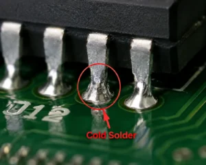
- Control the steps to aviod assembly mistake, such as chip direction, LED color, cold solder joints, to prevent quality problems during batch.
Detailed PCB First Article Inspection Process

A robust pcb first article inspection process is purposeful and methodical. Here’s an expanded look at standard steps:
1. Review and Planning
- Before first article produce, we will check the drawing, Gerber file , layour and bom list, to ensure all docuemnts are correct and no missing.
- For every features, such as layer count, pcb technology, customer’s requirement, we will customize a special FAI checking list, to control all process.
- We have a very professional engineering team, they all have many years experience, they always detect each steps, especially the quality team, to keep our professional and realiablity.
2. Controlled First Production Run
- We will follow the required material, components original&replacement,assembly standard, to make the first article, and once the first article confirmed, for mass prdocution, we will strictly follow everything same with the first article.
- Record every process and details, include the equipment parameter, Reflow soldering temperature range,PCBA assembly process and the operations. Establish a special docuemnts, keep a complete and traceable basis for verifying the effectiveness of mass production.
3. Inspection of the First Article
- Dimensional Inspection: Our inspect team will use original drawing and pcb specification, and measure tools with AOI automated optical inspection equipment to measure the ket dimension accurately, especiall the board size, hole size, pad space&size. To keep them cully match the standard and requirement.
- Solder and Assembly Inspection: Use 3D SPI solder paste inspection equipment and reflow soldering temperature zone data logs, to validate strictly with the height, volume and solder joint, at the sametime, we will do manually review and automated inspection, to confirm the assembly position, direction are correct. Cut the risk from the begining.
- Functionality and Electrical Tests: The first article use a power-on test to verify the main electrical parameters such as voltage, resistance, and current are correct, if need additional test, we will do a ICT or functional testing, to confirm the product’s phusical function and meet the customer’s design.
4. Documentation of Results
- We will make a detailed report, it include all components part number, deviations, pictures, tolerance, results, to keep the traceability..
- The report documents include allaspect of the assembly, if needed in mass production or futrue checking, we can know all details very easily, it also need to be signed by customer and inspection team.
5. Corrective Actions (If Needed)
- If we found the first article have any deviation, it will be recorded immediately and tracked back to analyse, the quality engineer will develop a corrective plan, calibrating the process parameter, evaluating the design, or updating process documentation. Mass production will only commence after the problem is resolved.
6. Approval and Process Control
- Only after all corrections and documentation are accepted does the PCB manufacturer receive the green light for mass production, locking in the process of record.
First Article Inspection Techniques & Tools
The inspection process for FAI incorporates a wide range of advanced techniques to check that boards meet every requirement. These include:
- Automated Optical Inspection (AOI): Use the tool toaccurate for component placement , orientation, and solder joint inspection.
- 3D Solder Paste Inspection (SPI): To check the solder paste whether in correct position, and check the amount.
- X-Ray Inspection: This is very important to check the hidied deatures, such as BGA or connectivity.
- Functional and In-Circuit Testing (ICT): Power-up the PCB, evaluate the signal, communication and load function.
- Manual Inspection by Quality Engineer: Inspect the appearance manually, stencil, and missing elements from the machine, to ensure every step have been checked with quality.
What’s Checked in a PCB First Article
Here’s a more detailed table of checks performed during a typical FAI:
| Area | What’s Verified | Tools Used | FAI Benefit |
| Dimensions | PCB length, width, thickness, hole location | Calipers, AOI machines, CMM | All boards meet stack-up and enclosure specs |
| Solder & Assembly | Solder joints, bridges, cold joints | Visual, AOI, SPI, X-ray | Prevents latent defects from poor soldering process |
| Electrical/Functional | Circuit function, test points, tolerances | ICT, functional testers, Multimeter | Boards operate to specified requirements |
| Material/Part Validation | Correct BOM and lot, trace codes | Trace software, manual check | Avoids wrong or counterfeit electronic components |
| Assembly Drawings | Consistency with PCB design and assembly | Engineering & operator review | Ensures process meets layout design and drawings |
FAI and the Assembly Process: How FAI Improves Quality

The pcb assembly processand first article inspection are intertwined. FAI isn’t just a stand-alone step; it is embedded within the assembly process to provide confidence in each process stage:
- Solder Paste Application: Use 3D SPI to check the solder past ampunt and position whether is correct.
- Pick-and-Place and Reflow: It is very important to inspect the PCBA after assembly, through the AOI equipment, and record the reflow oven profiles are logged .
- Post-Solder Inspection: After reflow soldering process, inspect every pcb board, to check the solder bridges, tombostoning, insufficient solder, etc.
- Final Test and Quality Engineer Review: After all process been inspected, we need to use ICT to test the function one by one, the quality engineer will confirm all data are recorded without other defects.
- Production Process Control: FAI locks in the process parameters. Once accepted, subsequent boards must follow the same procedures, with documented process controls, guaranteeing every PCB produced maintains top product quality.
Why This Matters
We can find the problems in time through the FAI process, then we can sove the issues from the source, to ensure each critical step, yielding a more stable production line.
Examples, Case Studies, and Common Issues
Example: Manufacturing Issue Solved by FAI
In our experience, we have produced a medical device, it’s very high-precision with a very narrow BGS. In the first article inspection, the engineer team found one conenctor was moved by 0.2mm, causing a problem. Because this problem was founded in first article, we re-check the first article and re-solder. In this way, a very big problem have been avoided, and maintaining the customer’s trust.
Common Issues Revealed by FAI
- Solder Paste Application Defects Uneven or insufficient solder on pads leads to open circuits or reliability problems. Early detection during FAI using SPI allows quick stencil or process adjustment.
- BOM or Part Mix-Ups Sometimes two resistor values are swapped in the supply chain. BOM traceability during FAI flags this before it causes hidden field failures.
- Reflow Soldering Process Variability Oven settings that differ from documentation can result in cold or brittle solder joints. FAI thermal profile checks protect against long-term reliability issues.
- Silkscreen Errors or Labeling Issues Not functional but critical for downstream assembly and serviceability.
The Benefits of FAI for PCB Fabrication and Assembly
Instituting a thorough FAI process delivers both immediate and long-term advantages in electronics manufacturing:
Immediate Benefits
- Defects Caught Early: We can control the quality—such as bridges, opens, component orientation errors—these aspects can be solved before any real damage happens.
- Cost Savings: If we find the problems during the first article, the cost will be lower than all boards have assembled. In this way, we can reduce a lot of loss.
- Regulatory and Customer Assurance: Full FAI documentation and compliance gives customers, auditors, and regulatory bodies confidence that the manufacturing process is both repeatable and robust.
Long-Term Benefits
- Process Control and Corrective Action: Consistent FAI processes create a closed-loop system: issues found in one run are documented and controlled, preventing repeats.
- Predictable Product Quality: Once a process is validated by FAI, every subsequent board benefits from the same attention to detail and best practices.
- Faster Time-to-Market for PCB Prototypes: When you know your process is dialed in, product releases accelerate.
Best Practices: Making the Most of FAI

- Plan FAI Early Involve your PCB manufacturer in DFM reviews and thorough documentation before the first production run.
- Communicate Clearly Share your assembly drawings, layout design files, and test plans early. Alert your CM to any “critical step” or complex process requirements.
- Leverage the Right Tools Ensure your supplier uses a mix of visual inspection, AOI machines, SPI, functional testers, and X-ray as needed.
- Request Detailed Inspection Reports A good FAI inspection report will include measurements, visual and automated inspection data, defect logs, corrective actions, and approvals from both manufacturing and quality engineering.
- Iterate on Findings Use feedback from the first article to improve design, update documentation, and dial-in manufacturing process controls.
- Adopt Change Control Any engineering change should trigger a mini-FAI, even if it seems minor. This keeps your process and product in lockstep with customer and regulatory needs.
Frequently Asked Questions
Is FAI required for every build?
No, FAI is typically required for new designs, major revisions, or when the manufacturing process is significantly changed (new supplier, new machine, new layout design). However, periodic FAI can help maintain high standards in ongoing production.
What if my first article fails inspection?
That’s exactly what FAI is for! The manufacturer should address the root cause, make any needed corrections, conduct another FAI if necessary, and only move to full production when the pcb meets all specified requirements.
How do I know my PCB manufacturer has done a thorough FAI?
Ask for the full FAI inspection report, including data from all inspection tools, images, and process logs. Look for traceability to the BOM, signed approvals from quality engineers, and clear documentation of corrective actions.
Does FAI slow down production?
A well-executed FAI adds only a short amount of time to your first production run but can save weeks or months by preventing costly rework and field failures downstream.
Conclusion
The pcb first article inspection process is a pillar of professional, high-reliability electronics manufacturing. This thorough process—rooted in detailed inspection, smart use of technology, experienced inspection teams, and full documentation—ensures that your first articles and every pcb that follows are built to exacting quality standards. By investing in robust FAI strategies, you catch defects early, lock in process and first article inspection best practices, and build a foundation for successful, repeatable production and customer satisfaction.
Working with a leading PCB manufacturer who offers first article inspection and leverages a blend of manual and automated inspection techniques is key to a successful, high-quality run of circuit boards—no matter how simple or complex the process.
Ready to get started or upgrade your FAI process?
Contact our quality engineer and inspection team for a free consultation, review of your PCB fabrication and assembly drawings, or to request a sample FAI inspection report today. Your next board deserves to be your best one yet.