
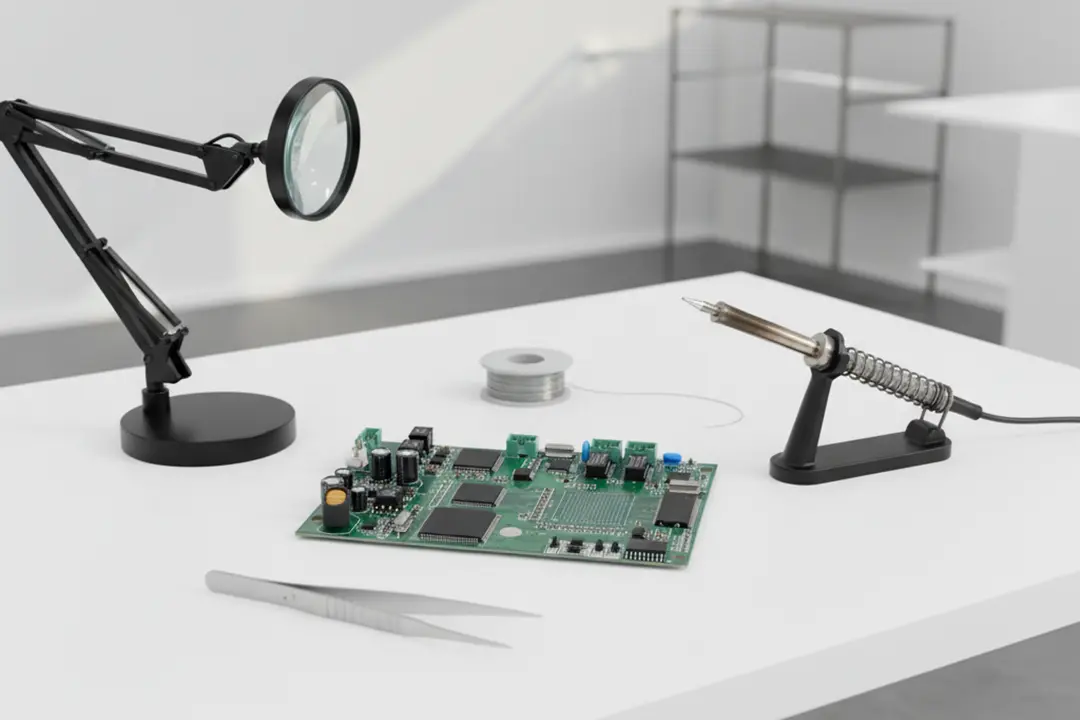
Introduction to Medical PCBs
Medical PCBs (printed circuit boards for medical purposes) are the core foundation of all modern medical equipment. From MRI magnetic resonance imaging and ultrasound diagnostic systems to portable blood glucose meters and wearable electrocardiogram monitoring devices, the performance of medical electronic products directly depends on the design capabilities of their built-in circuit boards, substrate selection, assembly processes, and manufacturing standards. We are well aware of the extremely high requirements for reliability, safety and precision in medical PCBS. From the high insulation and biocompatibility of PCB laminate materials to the one-stop service of cleanliness control and traceability system during the manufacturing process, LHD TECH integrates medical-grade standards throughout the entire life cycle of each PCB. It also enables us to become a reliable partner behind global medical equipment innovation with professional medical PCB solutions.
What Makes a Medical PCB Different?
Medical PCBS are far beyond the reach of ordinary circuit boards. It is a highly complex multi-layer printed circuit board specially designed and manufactured for the medical field, aiming to meet the highest standards of quality and reliability in the medical industry. Medical PCBS serve precise and accurate medical applications. Their core mission is to ensure patient safety and strictly adhere to regulations and standards worldwide. In fact, in the field of electronic circuit design and manufacturing, the medical industry is one of the most strictly regulated sectors. Every medical PCB we create, from the selection of laminating materials, circuit design to assembly process, adheres to the highest standards of patient safety and regulatory compliance. Facing international standards such as FDA, MDR, and ISO 13485, we integrate risk management and full-process traceability into our manufacturing system.
Why High-Quality Medical PCB Solutions Matter

Medical PCB solutions are the core support for the stable performance of medical electrical equipment used daily in hospitals, clinics and laboratories. Designing a high-quality medical PCB is far more than just achieving miniaturization or functional integration – its true essence lies in reliability, patient safety and regulatory compliance.This is also the uncompromising cornerstone of our manufacturing of medical PCB solutions.
Key Reasons Medical PCBs Must Meet the Highest Standards
- Patient Safety: For life support and treatment medical devices such as heart monitors and infusion pumps, as the core of the electronic system, the design and manufacture of PCBS must incorporate Failure Mode and Effects Analysis (FMEA) throughout to ensure a safe state even under a single failure condition.
- Reliability Requirements: Medical equipment typically needs to maintain continuous operation for several years or even over a decade, and is often exposed to harsh conditions such as repeated sterilization, high humidity environments, mechanical shock, or strong electromagnetic interference. Medical PCBS must possess excellent anti-aging, environmental resistance and electromagnetic compatibility (EMC) capabilities.
- Regulations of Medical Devices: The medical electronics field is strictly constrained by regulations such as ISO 13485, FDA 21 CFR Part 820, and IEC 60601. These regulations not only control the design and assembly process of PCBS, but also impose mandatory requirements on the traceability of components used, material composition, manufacturing environment (such as cleanliness), and documentation records.
- Data Security: Medical devices need to ensure the secure collection, encrypted transmission and complete storage of patient data. Medical PCBS must integrate signal integrity control, anti-interference layout and hardware-level security modules at the design level to prevent data loss, delay or illegal tampering, and ensure the authenticity and reliability of information.
- Support for Medical Research: Research-grade medical equipment (such as gene analyzers, high-precision imaging systems, and physiological signal acquisition platforms for experiments) has extremely high requirements for the repeatability, accuracy, and low noise of PCBS. Reliable medical PCBs should be capable of providing researchers with a stable electrical platform and more favorable data.
Circuit Boards and Circuits in Medical Equipment

Every medical device is powered by at least one circuit board—or, in the case of complex equipment, multiple interconnected printed circuit boards designed for specialized functions.
Circuits Used in Medical Devices
- Signal Processing Circuits: The weak physiological signals input by the sensor are filtered, denoised, programmable amplified and subjected to high-precision analog-to-digital conversion (ADC), providing a high-fidelity and low-distortion data foundation for digital signal processing and clinical diagnosis.
- Power Management Circuits: It provides multi-channel regulated output, low-ripple power supply and dynamic load response for microcontrollers, sensors, actuators and other loads, ensuring stable voltage and optimal energy efficiency of the system under all operating conditions, and meeting the electromagnetic compatibility requirements of medical equipment.
- Communication Circuits: Supports Wi-Fi, Bluetooth, Sub-1GHz or medical-specific wireless protocols to achieve secure and low-latency data interaction between medical devices and hospital information systems (HIS), electronic medical records (EMR), and remote monitoring platforms.
- Safety and Redundancy Circuits: Real-time monitoring of overcurrent, overheating, abnormal voltage and faults of key components, actively triggering backup path switching, power limiting or audible and visual alarms, enables the equipment to safely downgrade or orderly shut down under abnormal conditions, meeting the mandatory fail-safe requirements for medical equipment.
Medical electronic circuit design must strictly adhere to principles such as the separation of analog and digital signals, refined routing strategies, multi-level power zone planning, and highly effective electromagnetic interference (EMI) shielding – especially in medical imaging (such as CT, MRI, ultrasound) and diagnostic equipment Any signal crosstalk, power supply noise or ground bounce effect may directly reduce image quality or lead to incorrect measurements, thereby affecting clinical judgment and patient safety.
Medical Device Requirements & Regulatory Standards
Ensuring medical electrical equipment operates safely is a top priority, and regulations of medical PCB manufacturing are rigorous.
Must-Know Medical Field Standards
| Standard | Description/Applicability |
| ISO 13485 | Quality Management System for medical devices (regulates medical PCB manufacturing process) |
| FDA 21 CFR Part 820 | US regulation for quality system (QMS) requirements of device manufacturers |
| CE Marking | Compliance with European medical device guidelines |
| IPC Class 3 | Highest standards for electronics in critical applications (used in medical, aerospace, defense) |
| RoHS/REACH | Restricts hazardous substances in electronic medical equipment |
Requirements for PCB and Design for Manufacturing
- Traceability and Lot Tracking for every component and every batch of medical PCBs assembled.
- Full Documentation for each step, from schematic to final test report.
- Material Control: Only approved PCB laminate materials and solder types are used.
- Test Points: Test points are mandatory for all critical circuits to facilitate end-of-line and field testing.
Types of PCBs Used in Medical Applications
Not all types of PCBs are equal when working on medical electrical equipment. Each class of medical device has its preferred type of PCB based on function, complexity, reliability, and physical constraints.
Most Common PCBs for Medical Devices
| Type of PCB | Description | Used in Medical Devices Like |
| Single Layer | Simple, low-cost PCBs | Blood pressure cuffs, basic alarms |
| Double Layer | Twice the routing & component density | Portable glucose meters, basic diagnostic tools |
| Multilayer | 4–16+ layers, high density, high reliability | MRI & CT scanners, laboratory equipment |
| Rigid PCBs | Sturdy, not flexible, long-lasting | Medical imaging computers, diagnostic equipment |
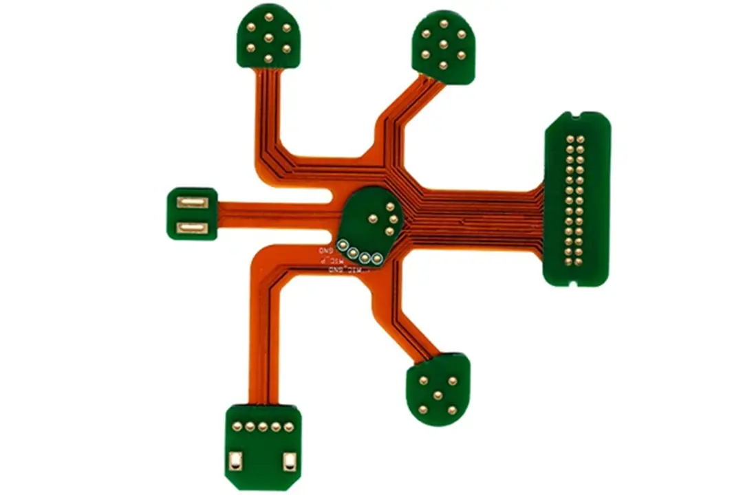
| Rigid-Flex PCBs | Combines rigid and flexible zones | Pacemakers, surgical instruments, wearable monitors |
| Flexible PCBs | Ultra-thin, bendable, fit in small packages | Smart patches, implantables, ear-worn monitoring |
| HDI PCBs | High Density Interconnect, microvias | Miniaturized devices, next-gen wearables, IoT medical |
| Ceramic PCBs | High thermal and chemical resistance | RF ablation systems, high-frequency oncology tools |
Key Consideration
For high-performance of medical electrical equipment, always use rigid-flex PCBs or HDI PCBs in compact, high-reliability, or wearable applications.
HDI PCBs: High-Density Solutions for Compact Medical Devices

The drive towards compact medical devices like wearables, subcutaneous monitors, and mobile scanners necessitates HDI PCBs—High Density Interconnect printed circuit boards.
Why HDI PCBs Lead in Modern Medical Devices
- Miniaturization: Through the HDI architecture featuring microvias, laser-drilled blind holes/buried holes, and ultra-fine wires (≤50µm), higher wiring density can be achieved within a limited area. This makes HDI PCBS an ideal carrier for miniaturized and lightweight medical devices such as portable monitors, wearable medical patches, implantable devices and handheld diagnostic tools, releasing more functional integration space for products.
- Performance: The advanced HDI design effectively supports high-speed data transmission (such as LVDS, MIPI interfaces), low-noise analog front ends and enhanced electromagnetic compatibility (EMC) structures. By optimizing the stacking structure and shortening the signal path, HDI PCB significantly reduces signal reflection and crosstalk, ensuring the accuracy and real-time performance of data acquisition in devices with extremely high requirements for signal-to-noise ratio and image quality, such as CT, MRI, and ultrasound imaging.
- Reliability: The HDI architecture adopts blind/buried vias instead of through vias, significantly reducing the number of welded nodes and via tail suspensions. Shorter interconnection paths and better return path designs enhance signal integrity (SI) and power integrity (PI). These characteristics directly meet the strict requirements of medical PCBS for long-term service life, anti-vibration reliability and electrical stability.
Advantages of HDI PCBs in the Medical Field
- Superior Electrical Performance: HDI PCB enhances signal fidelity and anti-interference capability by shortening the signal path, reducing parasitic capacitance and inductance, and incorporating an internal controllable impedance structure. It provides the best choice for medical devices that are extremely sensitive to signals, such as electrocardiogram monitors, medical imaging equipment (such as ultrasound, CT), diagnostic instruments, etc.
- Flexible Layout for Dense Functionality: HDI PCB supports the realization of multi-system integrated design within a compact single board – efficiently integrating functional modules such as sensor acquisition, signal conditioning, data processing, and wireless communication, meeting the dual requirements of medical equipment for the simultaneous development of miniaturization and multi-functionality.
- Enhanced Reliability: With fewer layers and fewer interconnection nodes (such as blind/buried vias replacing through vias), HDI PCBS structurally reduce the number of potential failure points, thereby lowering the risk of failure such as solder joint cracking and via fatigue.
- Support for Design for Manufacturing: The regularized layout and standardized process window of HDI PCBS make them more suitable for high-speed automated surface mount, reflow soldering and online inspection (AOI/AXI) processes, significantly improving assembly efficiency and first-time yield. Its design refers to the requirements of medical quality systems such as ISO 13485 and FDA 21 CFR Part 820.
IPC Class 3 and Other Reliability Standards
IPC Class 3 is the core specification for the design and manufacture of high-reliability electronic products, directly determining the performance and safety of medical electrical equipment. For medical devices closely related to patients’ life safety, such as implantable devices, wearable monitors, and life support systems, it is mandatory that their PCBS must comply with IPC Class 3 standards.
What is IPC Class 3?
- IPC (Institute for Printed Circuits): Formulate and maintain authoritative quality standards in the field of electronic manufacturing, including IPC-A-600 (Printed Circuit Board Acceptability) and IPC-A-610 (Electronic component Acceptability). These standards are applicable to critical application scenarios that require continuous operation, zero failure or uninterrupted performance.
- Class 3: Representing the highest level of reliability requirements, it is suitable for products that operate continuously at high performance or respond immediately on demand. At this level, the PCB must remain functionally intact and electrically stable under extreme environments, long-term service, and single failure conditions. Typical application fields include: medical equipment, aerospace systems, and military electronic equipment.
| Standard | Description | Used in Medical? |
| Class 1 | General electronics | No |
| Class 2 | Dedicated-service electronics | Sometimes, rarely |
| Class 3 | High-reliability, life-critical electronics | Yes (most medical PCBs) |
Important: Only partner with a pcb manufacturer that has proven expertise in manufacturing IPC Class 3 PCBs for the medical industry.
Design and Manufacturing: From Concept to Reliable Medical PCBs

Designing and manufacturing medical PCBs involves strict processes to ensure the highest standards are met from concept to finished circuit board.
Key Steps in Medical PCB Design and Manufacturing
Define Requirements for PCB and Medical Device
Design requirements in four directions: functional module division, interface definition, external dimensions and installation methods. At the same time, it is necessary to meet the performance indicators of signal accuracy, power consumption range, response time and anti-interference level. The product is used in different environments such as sterilization methods, working temperature and humidity, vibration and electromagnetic fields.
PCB Design and Schematic Capture
The design team should be led by a designer with medical PCB experience, familiar with high-reliability wiring rules and medical-grade DFM requirements. Ensure that signal integrity (SI), electromagnetic interference (EMI), and power integrity (PI) simulations are completed before the board is put into operation, and identify and optimize key networks. Internal cross-departmental reviews (hardware, manufacturing, testing, regulations) are conducted to ensure that the design is manufacturable and compliant.
Component Selection and Bill of Materials (BOM)
All components must have medical application ratings (such as compatibility certificates for AEC-Q100/Q200 and ISO 13485), and their sources must be traceable. Procurement is only made from the original factory, authorized agents or distributors that have passed strict reviews, and counterfeit or refurbished materials are strictly prohibited.
PCB Laminate and Material Selection
Choose the right pcb laminate materials High Tg FR-4 (≥170°C) is used in conventional medical electronics with good heat resistance and mechanical strength, and the cost is controllable.Polyimide flexible/rigid-flex composite board, used in wearable devices, features excellent flexural life, high-temperature resistance and radiation resistance. Ceramic substrates are used in implantable devices, featuring high thermal conductivity for high-power radio frequency, low dielectric loss, and excellent biocompatibility. At the same time, evaluate medical-specific requirements such as sterilization tolerance, flexural life, and biocompatibility (ISO 10993).
Prototyping and PCB Assembly
Rapid prototyping adopts a short lead time and small-batch trial production process to produce functional verification boards. Functional and regulatory testing is used for prototypes to conduct electrical performance, electromagnetic compatibility, safety regulations and reliability baseline tests. After the prototype is verified, small-scale trial production is carried out for preclinical evaluation or registration testing. After confirming that the process is stable and the yield rate meets the standards, smoothly transition to medium-batch and even large-scale production.
PCB Manufacturing and Assembly
- According to the ISO 14644 standard, the medical PCB manufacturing and assembly area must meet the ISO Class 7 or higher cleanliness level (such as Class 6) cleanroom requirements. Deploy ANSI/ESD S20.20-certified electrostatic protection measures throughout the entire process. Deploy online 3D AOI in the bare board manufacturing and PCBA assembly stages to meet the acceptability requirements of IPC-A-610 Class 3.
- Soldering (reflow and selective): Reflow soldering is used for SMT mounting, featuring a nitrogen-protected reflow oven to reduce oxidation and enhance the wettability of solder joints. Selective wave soldering is designed for THT through-hole and hybrid assembly boards, using selective soldering equipment to precisely control the flux spraying and soldering time.
- Surface Mount Technology (SMT) and Through-Hole Technology (THT) Surface mount technology (SMT) is suitable for high-density and miniaturized designs, using high-speed placement machines and high-precision mounting. Through-hole mounting (THT) technology is used for components that require mechanical strength or high current-carrying capacity, providing stronger solder joint anti-peeling performance. Most medical PCBS incorporate both SMT and THT components. We adopt a process sequence of “SMT reflow soldering first, followed by selective wave soldering”.
Inspection, Electrical Testing, and Functional Verification
After the medical PCB is assembled (PCBA), it must undergo 100% full inspection, covering three dimensions: appearance, internal structure and electrical performance. LHD TECH deploons a multi-level detection system in accordance with IPC-A-610 Class 3 and the specific requirements of medical equipment customers:
- Automatic Optical Inspection (AOI) : Online 3D AOI covers all assembly boards to detect surface defects such as solder joint morphology, device polarity, mounting offset, bridging/insufficient solder.
- X-ray Inspection (AXI) : For bottom pins or hidden solder joints of BGA, QFN, LGA, CSP, etc., 2D/3D X-ray imaging systems are used to automatically analyze void rate, solder distribution, bridging and cold soldering defects.
- Electrical and Functional Testing: Online Testing (ICT)/ High-voltage Insulation Testing (Hi-Pot0)/ Functional Testing (FCT)
Certification and Documentation
The production and testing process of each batch of medical PCBS must form a complete, traceable and controlled documentation package to support customer regulatory reviews, post-market supervision and potential recalls or on-site maintenance. Batch record contents include: material entry inspection reports, process control parameters, inspection data of each process, special process records, and maintenance and rework records. Compliance documentation including ISO 13485 the corresponding quality record, DHF/DMR/DHR/CMRT/REACH/ROSH.
Best Practices for High-Quality Medical PCB Solutions
- Design for Automated Inspection (DFT) : To ensure that medical PCBS can perform AOI, AXI and ICT inspections efficiently and accurately after assembly, the design stage must systematically embed inspection assistance features: optical positioning points (fiducials)/clear silk-screen marking/dedicated test point layout.
- Redundant power and ground plane design: For medical electronic systems with extremely high reliability requirements such as life support, intensive care, and surgical equipment, PCBS must achieve a redundant architecture for power and ground planes: multi-layer redundant planes/low-impedance loops/thermal and current balancing.
- Full-process version-controlled documentation system: At every stage from the design to mass production of medical PCBS, a strict version management and documentation record mechanism must be established to support the requirements of regulations such as ISO 13485 and FDA 21 CFR Part 820 for design history files (DHF) and device master records (DMR). Version-controlled drawing/layout file management /BOM version control/test log archiving.
- Dual verification: Simulation analysis and real environment functional testing. Before medical PCBS enter mass production, they must undergo dual verification through simulation verification and actual working condition testing to ensure that the design theory is consistent with the actual performance: simulation verification/real environment functional testing/closed-loop optimization.
Test Points, Inspection, and Quality Assurance in Medical PCB Assembly
A reliable pcb assembly process requires stringent quality assurance steps.
The Role of Test Points in Medical PCBs
- Accessible Debugging: Test points offer a way to probe and verify crucial signals, voltages, and functionality without damaging the medical device.
- Ongoing Maintenance: Allow for in-field testing and easy troubleshooting of devices without disassembly.
Inspection Points and Quality Metrics
- Automated Visual Inspection (AOI): It can quickly and accurately identify surface mount defects. Detect problems and defects such as solder Bridges, missing components, incorrect polarity, erected monuments, offsets, and insufficient solder. We adopt online 3D AOI, in combination with high-resolution cameras and multi-angle light sources, to achieve a defect detection rate of ≥5%, and all inspection images and data are automatically uploaded to the MES system.
- Electrical Test: The connectivity of the PCB network and the correctness of component parameters can be verified. Core verification items: on-off test/component value verification/insulation resistance test.
- X-Ray Inspection: Non-destructive X-ray inspection of hidden solder joints and internal structures is particularly suitable for high-density and HDI PCBS. Necessity: Blind/buried vias/inner layer defects of multi-layer boards in bottom pin devices such as BGA/CSP/QFN /HDI boards. It can be equipped with 2D/3D X-ray systems to perform 100% critical area inspection on medical PCBS, and the BGA cavity rate is strictly controlled at ≤15%.
- Environmental Stress Screening: It can identify potential defects that may occur during the early use of the product and enhance on-site reliability. Method combination: Rapid temperature cycling/damp heat exposure/random vibration. ESS is regarded as an optional or mandatory process for medical high-reliability products. The finished boards are batch-sampled or fully screened through a three-combination test chamber of temperature, humidity and vibration.
Quality Metrics (Typical for Medical PCBs)
| Metric | Target Value |
| PCB Failure Rate | <50 ppm (parts per million) |
| Solder Joint Defects | <1 / 10,000 |
| Traceability | 100% lot and batch traceable |
| Compliance | Class 3, ISO 13485, RoHS |
Applications for Medical PCBs in Healthcare and Medical Technology
Medical PCBs are present in nearly every aspect of healthcare and medical applications. Here are some of the most important:
Major Applications in Modern Medical Devices
- Medical Imaging: The covered equipment includes MRI (Magnetic resonance Imaging), ultrasound diagnostic systems, CT scanners, and X-ray computed tomography. We offer HDI rigid plates that meet medical imaging standards, supporting advanced processes such as embedding resistance and capacitance, back drilling, and local mixed pressure, to help imaging equipment achieve clearer clinical images.
- Mobile Health and Wearable PCBs: Smartwatches, health monitoring patches, subcutaneous sensors. PCB requirements include compact flexible/rigid-flex boards/low-power signal layers/high-density interconnections. Our medical-grade flexible PCB supports a bending radius of ≤5mm and a bending life of ≥ 100,000 times, serving as a reliable interconnection foundation for wearable health devices.
- Diagnostic Equipment: Blood glucose monitors, blood pressure monitors, portable electrocardiogram machines (ECG). Commonly used PCBS: double-layer/multi-layer boards /HDI or ceramic substrates/anti-interference design. Diagnostic grade PCBS, through strict impedance control and noise testing, facilitate the wide deployment of rapid and reliable point-of-care testing (POCT) devices.
- Life-Support & Implantables: Pacemaker, infusion pump, ventilator. Commonly used PCBS: rigid-flex boards/ceramic substrates/advanced reliable types that comply with IPC Class 3 and ISO 13485. Life support grade PCBS strictly undergo 100% electrical testing, X-ray inspection and environmental stress screening.
- Hospital Networks and Communication: Nurse call/alarm system, patient monitoring terminal, wireless communication interface. PCB technical requirements: Robust standardized PCB (using FR-4 substrate and conventional process)/Reliable connection and anti-interference (enhanced power integrity and EMC design)/maintainability design (standardized interfaces, test points).
- Medical Research and Laboratory Automation: Analytical instruments, sample preparation systems, gene sequencers.PCB technical requirements: High-precision analog circuits/high-speed digital interfaces/scalable modular design. We support special processes such as ceramics and high-frequency mixed pressing.
Selecting the Right PCB Manufacturer for Medical PCB Solutions
Choosing a pcb manufacturer experienced in the medical sector is key for successful medical device manufacturing.
Key Factors to Look for in a PCB Manufacturer
- Certification: The manufacturer must hold ISO 13485 (Medical Device Quality Management System), ISO 9001 (General Quality Management), and possess necessary certifications such as the CE mark (EU compliance) and FDA registration (US market access).
- Class 3 Expertise: It is necessary to verify the manufacturer’s practical experience and batch delivery records in the field of medical-grade PCBS, and confirm that it has the ability to design, manufacture and inspect in accordance with IPC Class 3 standards, including comprehensive control over materials, processes, testing and documentation.
- Advanced Capabilities: It should have the mass production capacity of various circuit boards such as HDI (High-density Interconnect), rigid-flex boards, ceramic substrates and high-frequency materials to support diverse demands ranging from implantable devices to medical imaging systems.
- Quality Control: The manufacturer must have core inspection equipment such as internal AOI (Automatic Optical Inspection), X-ray inspection (AXI), and environmental stress screening (ESS), and operate a documented quality management system (QMS).
- Supply Chain Management: Traceable procurement channels for materials (such as UL-certified base materials and medical-grade components) should be established, and dual-source/multi-source alternative material lists should be maintained to cope with supply chain fluctuations and ensure continuous delivery capabilities.
- Design for Manufacturing Support: The manufacturer’s engineering team should be able to participate in design reviews, provide optimization suggestions for mass production, traceability and regulatory compliance, reduce manufacturing risks from the source and shorten the product launch cycle.
- Full Documentation and Traceability: It is necessary to be capable of providing complete records from raw material batches, process parameters, test results to the serial numbers of finished boards, supporting customer audits, post-market supervision, and potential recall or on-site maintenance requirements.
Future Trends: Reliable, Miniaturized, and Smart Medical PCBs
Advances in medical technology are taking the performance of medical printed circuit boards to the next level.
Key Trends in Medical PCB Solutions
- Miniaturization and System-in-Package: Through high-density interconnect (HDI) PCBS, sensors, microprocessors, power management units and wireless communication modules are integrated on a single substrate, achieving a high degree of functional integration and maximum space utilization.
- Flexible, Wearable, and Even Ingestible PCBs: The advancement of flexible electronics technology has given rise to flexible, stretchable and biocompatible circuit board forms, supporting innovative applications such as continuous physiological monitoring, intelligent diagnostic patches and disposable micro endoscopes.
- Edge Computing and AI Integration: The advancement of flexible electronics technology has given rise to flexible, stretchable and biocompatible circuit board forms, supporting innovative applications such as continuous physiological monitoring, intelligent diagnostic patches and disposable micro endoscopes.
- Sustainable PCB Manufacturing: Medical PCBS are gradually integrating microcontrollers or AI coprocessors, enabling tasks such as signal processing, feature extraction, pre-diagnosis, and data compression to be completed directly on the circuit board. This architecture significantly reduces data transmission latency and alleviates cloud load.
- Cybersecurity at the Hardware Level: The medical industry is accelerating its transformation towards green production, adopting halogen-free, lead-free and Rohs-compliant laminated materials, and optimizing the use of energy and chemicals in the manufacturing process to reduce the environmental impact of electronic medical waste.
- Bio-Compatible and Smart Materials: With the integration of medical devices into the Internet of Things (IoMT), PCB design has begun to incorporate hardware-level protection measures such as security elements (SE), encryption modules, and physical unclonable functions (PUF), to resist cyber attacks from the source, protect patient privacy data, and meet the latest medical device cybersecurity regulations such as those of the FDA and the EU MDR.
Conclusion: Making Medical Devices Safer with Reliable Medical PCBs
Medical PCBs—From the simplest single-layer boards to the most complex HDI and rigid-flex designs, medical PCBS form the invisible cornerstone of almost all modern medical equipment. Its reliability, quality level and compliance grade not only determine the performance of medical equipment, but also directly relate to the safety, effectiveness and clinical outcomes of today’s medical applications.
Key Takeaways
- Medical PCB solutions help create a safer, smarter and more efficient medical service system by providing engineers and innovators with the basic modules needed to build modern medical technologies.
- The medical device manufacturing process is subject to extremely strict regulatory supervision: Only PCB manufacturing systems that adhere to the most rigorous process standards and operate the most controlled supply chain are qualified to produce medical-grade circuit boards.
- Choosing a professional medical PCB manufacturer as a partner can ensure the consistency of product quality, the certainty of regulatory compliance, and obtain the application support of the latest innovative achievements in the PCB field in the first place.
Final Tips for Success
- Always specify IPC class 3 or higher for critical or implantable medical applications.
- Choose a partner experienced in the regulations of medical device design and able to provide medical PCB assembly, board traceability, and complete documentation.
- Prototype early, test under real-world operating and sterilization cycles, and keep your supply chain robust with dual or triple sourcing of components.
- Focus on design for manufacturing—involve your PCB manufacturer’s engineering team as early as possible and leverage their expertise.