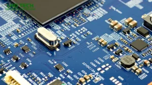
Introduction to High Frequency PCBs
High frequency PCBs—also known as high-frequency printed circuit board, high-frequency pcb or RF pcb, is indispensable in almost every field of modern high-speed electronic product. These circuit boards are designed to manage high-frequency signal, typically range from several hundred MHz to over 100 gigahertz (GHz). They are the backbone of communication system, demanding high-speed data transmission, minimal signal loss, and impeccable performance under various operate condition.
With the rise of 5G, Internet of Things and satellite communication application, the demand for high frequency has increased, posing new challenge for electronic engineer in designing high-frequency PCBs. High-frequency pcb design is not merely about connecting component; it is about managing complex electromagnetic effect, reducing noise, ensuring thermal stability, and choosing the right advanced material.
What are High-Frequency PCB Communication Circuits?
High-frequency PCB communication circuits are specially designed printed circuit boards for operation at high frequency, featuring low signal loss, minimal noise and high reliability. They support the transmission of high-frequency signal within the specified frequency range – process analog signal, RF (radio frequency) signal or high-speed digital waveform.
High-frequency circuit not only require meticulous layout and design, but also special material with low dielectric constant (Dk) and low dissipation factor (Df). The unique requirement of high-frequency PCB mean that every stage – component, routing, grounding, stacking, and even the selection of solder mask – is more important than ever.
Features of a High-Frequency Printed Circuit Board:
- Designed to sustain signal from 500 MHz into the GHz range.
- Utilize advanced material (PTFE, Rogers, ceramic-filled, or improved FR4) for low dielectric loss.
- Require careful control of trace impedance, tight clearances, and spacing.
- Emphasize consistent bandwidth and low signal degradation, even at the highest frequency.
High Frequency PCB vs. High Speed PCB
Often, high-frequency PCBs and high-speed PCBs are confused—but their differences are important for both design and manufacturing.
| Aspect | High Frequency PCB | High Speed PCB |
| Frequency Target | Analog/RF signals in MHz to 100+ GHz range | Digital signals, focused on rise time/edge rate |
| Key Concern | Controlled impedance, dielectric properties, EMI | Timing, skew, data integrity, jitter |
| Common Materials | PTFE, Rogers, ceramics, specialty RF laminates | High-grade FR4, sometimes Rogers |
| Primary App | RF comms, radar, satellite, wireless systems | Processors, memory, data backbone |
- HF PCB sare cycle-based (frequency domain): Focus is on the frequency characteristics, impedance, and filtering of analog/RF signal.
- High-speed PCBs are bit-rate-based (time domain): Focused on transmitting data with short rise times and minimal timing errors often below 5 GHz but at extreme edge speed.
Types and Application of High Frequency PCBs
Major Types:
Analog HF PCBs Used for analog/mixed-signal environments where analog performance and signal quality are paramount (e.g., medical device, high-sensitivity sensor).
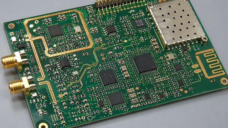
RF PCBs Used in wireless modules, Bluetooth/Wi-Fi, and 5G base stations.
Microwave PCBs Deployed in radar systems, satellite communication, point-to-point wireless, and aerospace.
Common High Frequency PCB Application
- Wireless communication systems (5G, Wi-Fi 6/7, LTE, Bluetooth).
- Radar system and microwave antenna.
- Data transmission and networking hardware.
- IoT and edge computing devices.
- Medical electronics and imaging.
- Aerospace and satellite PCB assemblies.
Core Features and Material Selection for High-Frequency PCBs
The unique demand of high frequency signal transmission mean that high-frequency PCBs must have certain advanced feature and use special material with low dielectric constant.
Essential Features
- Low Dielectric Constant (Dk): Minimizes signal delay and maintains impedance.
- Low Loss Tangent (Df): Reduce energy loss as heat (dissipation factor).
- High Thermal Conductivity: Prevent hot spot and makes board suited for high-power wireless communication.
- Low Moisture Absorption: Maintain dielectric performance in humid environment.
- Stable Coefficient of Thermal Expansion (CTE): Prevents warping from temperature swing, essential for multi-layer HF PCB.
- Dimensional Stability: Maintain exact distance/position between trace and layer.
PCB Materials for High-Frequency Application
| Material | Dielectric Constant (Dk) | Dissipation Factor (Df) | Application |
| PTFE (Teflon) | 2.0–2.5 | <0.0017 | Aerospace, microwave, radar |
| Rogers Laminate | 2.5–3.5 | 0.002–0.003 | RF comms, 5G, IoT, high-speed |
| Ceramic-Filled | 6–10 | <0.002 | Military, high-power microwave |
| Modified FR-4 | 3.9–4.5 | ~0.014 | Mixed analog/digital, low-end RF |
Major Challenges in Designing High Frequency PCBs

Designing high-frequency PCBs is a meticulous process filled with unique challenge that differentiate HF PCB design from conventional approach. PCBs are essential for ensuring stable, low-loss signal transmission—yet, signals at high frequency interact with every element of the layout, material, and PCB structure. Let’s review the most critical challenge:
Signal Integrity Issues
- Impedance Mismatch: Every section of a printed circuit board must be precisely controlled for impedance. Any discontinuity can cause reflections and signal loss, leading to degraded high-frequency signal quality.
- Crosstalk and Coupling: Trace running too close together can lead to capacitive and inductive coupling, especially at high frequency—a classic problem in dense PCB design.
- Harmonic Distortion: Parasitic effect within circuit board induce harmonic distortion, affecting the overall fidelity of analog and high-frequency signal.
- Common Mode Noise: Stray capacitance between trace or improper ground return can create noise, particularly in the power delivery network (PDN).
Electromagnetic Interference (EMI) & Electromagnetic Compatibility (EMC)
- OnboardEMI Emitters: Power supplies, oscillator, and converter on a high frequency board can radiate interference. EMI is especially critical in wireless communication PCBs used in shared, dense spectrum environment.
- External EMI Susceptibility: PCBs in communication system need EMI resilience—even nearby PCBs or devices can inject disruptive energy if EMC isn’t controlled during design.
Thermal Management
- Dissipation Factor & Losses: Materials must have a low Df and high thermal conductivity to ensure minimal signal loss and prevent overheating, especially for high-power RF and high-speed PCBs.
- Surface Tracking & Voltage: High voltage in dense, high frequency PCB applications may lead to surface tracking—insulation breakdown along the board that can cause system failure.
PCB Manufacturing Constraint
- Board Stackup Complexity: High frequency boards often combine multiple material(e.g. Rogers plus FR-4 layer) whose stackup and lamination tolerances must be strictly controlled.
- Microvia & HDI Requirement: At mmWave and high-speed, microvias, controlled depth drilling, and HDI process increase manufacturing complexity, requiring experienced fabricator.
Summary Table: High Frequency PCB Challenges
| Challenge | Cause/Effect | Solution |
| Signal Loss/Reflection | Impedance mismatch, via stub | Controlled impedance routing, backdrilling |
| Cross-talk | Traces too close | Adequate spacing, ground shielding |
| EMI/EMC Failure | Poor layout, inadequate shield | Shielding, via stitching, filtering |
| Overheating/Hot Spot | High Df, inadequate copper or via | Low Df substrate, thermal via |
| Moisture Absorption | Poor laminate choice, environmental exposure | Low-absorption material |
Design Guidelines for High Frequency PCB Communication Circuits

Smart Material Selection
- Prioritize low-Dk, low-Df material: PTFE, Rogers, and ceramic-filled substrate outperform standard FR4 for high frequency printed circuit board, minimizing signal loss in the frequency range of interest.
- Consistent Stackup: Build symmetrical PCB stackup to prevent warping due to CTE mismatch—a chief concern in advanced multi-layer high-frequency PCBs.
Layout and Routing Principles
- Trace Control: Route high-frequency signal transmission lines with calculated width and gap for precise impedance control. Use microstrip, stripline, or coplanar waveguide configuration for different section.
- Minimize Trace Lengths: Longer trace not only increase signal loss but also act as antenna, raising EMI risk.
- Differential Signaling: Use matched differential pair for high-speed data link, maintaining equal length for signal to minimize skew and common-mode noise.
- Isolation of High-Speed Regions: Spatially separate analog, digital, and RF zone to reduce coupling and parasitic interference.
Grounding and Shielding
- Solid Ground Plane: Place spacious, uninterrupted ground plane under high-frequency circuits to reduce EMI and enable accurate impedance control.
- Via Stitching & Fencing: Surround noisy sections with fence of ground via, providing vertical shielding and return path for current.
- Local Shield Cans: Enclose particularly sensitive or noisy component (RF IC, oscillator) within metal shield.
Power Integrity
- Decoupling Capacitors: Place broadband capacitor close to supply pins to shunt noise to ground and maintain power integrity for high-speed design.
- PDN Design: Simulate and optimize the entire power delivery network to prevent voltage droop and supply fluctuation during fast switching.
Filtering and PCB Constraints
- Strong Input Filtering: For fast switching application, filter both the signal and power entry point using on board passive network.
- Design Rule/Constraint Management: Use ECAD tools’ constraint setup to enforce the rules for clearance, matched pair, and maximum trace lengths from the start.
Best PCB Layout Practices for HF Circuit
Implement the following PCB layout best practice to achieve robust high-frequency signal quality and EMI/EMC compliance:
- Avoid 90-degree Trace Turns: Sharp angles serve as signal heat sinks. In high-frequency design, use 45-degree or curved traces to maintain signal integrity.
- Controlled Impedance Routing: Use precision tools to calculate and lock the trace impedance of all high-frequency or differential trace.
- Group Like Signal: Keep analog, digital, and RF traces grouped and separated to avoid cross-talk.
- Strategic Layer Assignment: Assign separate layers for high-speed and low-speed signal, and always sandwich high-frequency routes between solid ground or power plane.
- Thermal Via Array: For power amplifier or RF amplifier, a dense array of hot channel is used beneath the chip to transfer heat to the internal copper plane, preventing the formation of hot spot.
Testing, Troubleshooting, and Compliance
Key Testing Procedures
- Time Domain Reflectometry (TDR): Any discontinuity will cause reflection and signal loss, lead to a decline in the quality of high-frequency signal.
- Vector Network Analyzer (VNA): Scan the S-parameter on key transmission path for reflection/insertion loss verification of RF and microwave circuit board.
- Oscilloscopes: Directly verify the rise time, differential signal integrity, overshoot, jitter and crosstalk.
- Thermal Imaging: Identify thermal stress or hotspot during full-speed or high-power operation.
Compliance & PCB Manufacturing Standard
- IPC-6018: Set the standard for microwave/high frequency PCB manufacturing.
- IPC-2221 & 2223: Define the general design rules for high-speed, high-frequency PCB design and stack
- FCC, CE, IEC: Governing EMI/EMC emissions and susceptibility, absolutely necessary for market access.
Troubleshooting Example
- High loss at gigahertz frequency: Check whether the copper surface is rough, the Df does not meet the specification, or the length of the wire traces/through hole is too large.
- Unexpected EMI: Inspect for split ground plane, poor connector/launch design, or miss via fence.
PCB Manufacturing for High Frequency Boards

Special PCB Manufacturing Considerations
- Laminate Selection and Handling: High-frequency PCBS use special laminate that are sensitive to moisture and temperature. It is necessary to strictly control storage, lamination and drilling.
- Microvias and HDI: High frequency and small size are achieved through micro-hole and high-density interconnect (HDI) technology, which require precise laser drilling and advanced electroplate.
- Surface Finish: Usually, gold (ENIG) and silver finishes are chosen instead of HASL to maintain signal quality and corrosion resistance at high frequency.
- Quality Control and Test: Advanced automatic optical inspection (AOI), electrical testing and high-power aging testing confirm the integrity of the circuit board before assembly.
Future Trends in High Frequency PCB Design and Manufacturing
- Mixed Signal and Hybrid Stackups: Boards are increasingly integrating mixed-signal (digital + RF) paths, using Rogers material and advanced FR4 hybrid stacking to meet RF and high-speed digital requirement.
- Embedded Passives and Antennas: Integration of passive component and antenna inside the PCB itself is on the rise for IoT, mmWave, and miniaturized board.
- Flexible and Rigid-Flex HF PCBs: Wearable devices, medical equipment and aerospace now use flexible or rigid-flexible high-frequency PCBs to achieve bonding and high-frequency performance.
- Automated Design and Simulation: AI-powered PCB design software offer advanced DFM (Design for Manufacturability) feedback, constraint verification, and electromagnetic simulation to achieve faster and more reliable high-frequency circuit boards.
- Green, Recyclable Substrates: With the improvement of environmental protection standards, PCB manufacturing will emphasize halogen-free, low-emission and recyclable HF PCB material.
FAQs on High Frequency PCB Design
Q1: What is the main difference between high-frequency PCBs and traditional PCBs?
High-frequency PCBs are designed with low-loss and low-dielectric material and are used for signal transmission at frequency above 500 MHz, emphasizing signal integrity, EMI and impedance control.
Q2: Why are Rogers materials or PTFE preferred in high frequency applications?
They offer a stable dielectric constant, extremely low Df, low hygroscopicity and excellent thermal expansion performance – ideal for maintaining performance at high frequency.
Q3: Can FR-4 be used for high-frequency PCBs?
Advanced FR-4 can only be used in low and high-frequency application or non-critical signal path. True high-frequency PCB design rely on material specifically designed for GHz signal.
Q4: How to minimize EMI and achieve EMC compliance in high-frequency PCB design?
Use continuous ground plane, through splicing, appropriate shielding (such as metal “cans” and fence via), and carefully separate high-speed/high-frequency area. Strict PCB design rule are adopted for spacing and control impedance. Filters are used at each signal/power input, and the layout is verified through simulation tool dedicated to electromagnetic compatibility.
Q5: What factors most influence signal loss in high-frequency PCBs?
The biggest contributor to signal loss at high frequencies are:
- High dissipation factor (Df) in PCB material
- High dielectric constant (Dk) mismatches across substrates or layer
- Excessive trace length and unnecessary via
- Rough copper profile and poorly finished surface
- Moisture ingress and thermal expansion causing micro-delamination or dielectric shift
Q6: Why is the coefficient of thermal expansion (CTE) important in high-frequency PCB design?
Low and stable CTE ensure minimal dimensional change at the working temperature. This is crucial for aligning multi-layer board in manufacturing and maintaining consistent signal transmission, especially when PCBSs are used in demanding environment such as aerospace, automotive, and outdoor wireless application.
Q7: What is the role of impedance matching in the design of high-speed and high-frequency printed circuit board?
Impedance matching ensure the maximum transmission of signal power and reduce signal reflection at discontinuity. Controlling impedance routing, precise trace width/gap specification, and precisely designed PCB stacking are crucial for robust high-frequency signal transmission.
Q8: Are there any special considerations when assembling PCBS with high-frequency boards?
Yes. Component for high-frequency PCBs often have smaller, more sensitive footprints (like 0201/01005 passives or shielded RF packages) and may require mild assembly temperature to avoid laminate damage. Cleanliness during assembly is critical—any flux residue, solder ball, or foreign object can drastically affect signal integrity in a high-frequency, high-speed PCB.
Yes. Components used for high-frequency PCBS typically have smaller and more sensitive footprints (such as 0201/01005 passive or shielded RF packages), and may require a mild assembly temperature to prevent laminate damage. The cleanliness during the assembly process is of vital importance – any flux residue, solder balls or foreign objects can seriously affect the signal integrity in high-frequency and high-speed PCBS.
Conclusion
The development of electronic product – from high-frequency radar system and advanced wireless communication to everyday smart devices – absolutely relies on precise and reliable high-frequency PCB design and manufacturing. Today’s high-frequency PCBs are manufactured to strict standards, using low dielectric constant material, custom stacking and advanced layout techniques to ensure powerful performance at an increasing number of signal frequency.
The art and science of designing high-frequency circuit lie in anticipating and mitigating every potential source of signal loss, electromagnetic interference, resonance or thermal stress. PCBS can not only connect electronic component, but also maintain signal integrity, power integrity and electromagnetic compatibility over a wide frequency range.
Whether your application is communication satellites, next-generation 5G device, high-speed data centers or micro Internet of Things sensor, your path to success is paved with appropriate material selection, strict manufacturing practices and meticulous PCB layout. As the global demand for high-frequency and high-speed data transmission increases, those who invest in advanced PCB design and manufacturing will lead the future of electronic product.