Introduction to Printed Circuit Boards
You can hardly find a modern electronic device that doesn’t depend on a printed circuit board (PCB). Think of smartphones, industrial controllers, or even medical implants—their basic operation all comes back to a properly laid-out circuit board.
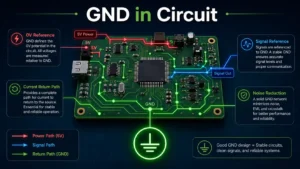
You ever wonder what a PCB really does? For one thing, it keeps all the little electronic bits from falling off. For another—and this is just as important—it gives them the electrical routes they need to connect and do their job. Take a typical PCB apart and you’ll see it’s built in layers: some insulating material, some copper foil, and a protective coating on top. Squish those together and you’ve got a tough, dependable circuit. That’s why PCBs are everywhere—from a simple TV remote all the way up to powerful servers.
The Basics of PCB Design & Composition

You might be laying out just a single side of the board for some simple IoT gadget. Or maybe you’re working with multilayer board inside a supercomputer. Either way, if you don’t get the basics of pcb design down, you’re in trouble.
How Printed Circuit Boards Are Made
Ever wonder what’s actually inside a PCB? It’s really just a few different materials working together. You’ve got insulators—fiberglass and epoxy resin, for instance. Then there’s a conductive layer, which is almost always copper foil. And on top of that, you add protective coatings like solder mask and silkscreen. They will laminate and bond these layers into a solid board during the manufacturing process, with each layer serving its own purpose
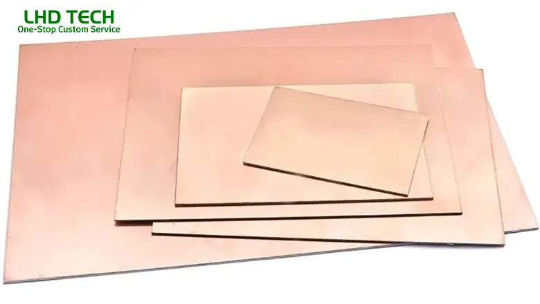
Take the substrate, or base material. That’s the main insulating board, usually made from fiberglass (FR4) mixed with epoxy resin—though sometimes you’ll see advanced ceramics or polyimide in there too. Then there’s the copper layer, which actually forms the electrical circuit. Usually, it’s just copper foil. Below is the solder mask, which is used to protect the copper underneath and prevent damage to the solder bridge during assembly. Behind it is silk screen printing, which is used to display instructions that match the label. During welding, the position of each component can be confirmed through silk screen printing, and some company logos can be displayed. For more advanced PCBs, a coating can be added to the top layer for protection, providing functions such as moisture resistance, dust prevention, and protection against other chemicals
Key Points:
- Every modern printed circuit is based on careful selection of board material.
- Good PCB design ensures all electronic components—resistors, capacitors, integrated circuits, connectors—are mounted securely and can perform at their best.
Types of PCBs: Rigid, Flexible, and Beyond
Printed circuit boards are made in several configurations, each serving different purposes across the electronics industry.
Types of PCBs
- Single-sided boards:
- Only one side copper.
- Normally using in simple product,like small toy.
- Double-sided boards:
- Simply words which is double copper layers.
- Through-holes connect circuits on both sides, supporting more complex designs.
- Multi-layer boards:
- Simply put which is more than two copper boards,which could be 4,6,8…
- Essential for computers, communication, and space-constrained devices.
- Rigid PCB:
- The standard; maintains a fixed shape.
- Rigid printed wiring board:
- Another term for rigid PCBs, emphasizing their use in wiring and structural roles.
- Flexible printed circuit (FPC):
- Made with polyimide substrate, allowing bending and folding.
- Used in wearables, cameras, and smartphones.
- Rigid-flex circuit boards:
- Combines rigid and flexible sections, commonly found in aerospace and medical devices.
- Metal core printed circuit:
- Uses a metal (usually aluminum) substrate for superior heat dissipation.
- Found in LED lighting and power electronics.
Types of PCBs
| Type of PCB | Substrate Material | Usage | Key Feature |
| Single-sided | FR4 | Simple electronics | Low cost, basic pcb |
| Double-sided | FR4 | Consumer devices | Routing on both sides |
| Multi-layer | FR4, ceramics, polyimide | Servers, computers, routers | High density, signal integrity |
| Rigid PCB | FR4, metal core | TV, computer, automotive | Stiff, strong |
| Flexible PCB | Polyimide | Wearables, foldable phones | Can bend, curve, flex |
| Rigid-flex | FR4 + polyimide | Aerospace, medical devices | Complex, dynamic |
| Metal core | Aluminum, copper | LEDs, power supplies | Heat dissipation |
PCB Substrate Materials: Choosing the Right Base

What Does “Substrate” Mean?
Substrate, every PCB has this thing called a substrate. There are many options to apply to different scenarios, such as special substrates to choose from when the bending degree of the circuit board needs to be softer, as well as temperature. For example, in environments that require long-term operation, there will be different substrate requirements. Choose a substrate that suits your product based on your needs.
Common Substrate Materials
- FR4 (fiberglass-reinforced epoxy):
- Most popular substrate for rigid boards.
- Balances cost, strength, and insulative properties.
- Polyimide:
- Used in flexible printed circuit boards.
- Excellent temperature and chemical resistance.
- Ceramic materials (aluminum oxide, aluminum nitride):
- Ideal for high-frequency, high-power, or harsh environments.
- Metal core (aluminum, copper):
- Used when heat must be dissipated rapidly (as in high-power LED applications).
Why the Substrate You Choose Actually Matters
There are too many points that are affected by the substrate, such as temperature scenarios, moisture-proof scenarios, chemical usage scenarios, indoor and outdoor scenarios. If the corresponding substrate is not selected, the product’s lifespan and usage frequency will be greatly reduced, which may also affect the company’s reputation.
Layers of a PCB Explained: Copper, Solder Mask, and More

A modern printed circuit consists of multiple layers, each serving a unique and essential function.
The Layers of a PCB (Layer Stack-Up)
Let’s break down what goes into a typical PCB, layer by layer.
First up, you’ve got the copper layers – these are the most critical ones because they actually carry the signals and power. A simple single-sided board has just one copper layer. Double-sided? Two. But if you’re dealing with a multi-layer board, you could have 16 or even more layers stacked up.
Underneath all that copper is the substrate – that’s the mechanical foundation. It’s usually made from insulating materials like FR4, polyimide, or ceramics. Basically, it holds everything together.
Then comes the solder mask. This is the layer that covers all those copper traces so you don’t accidentally create shorts when soldering. It also protects the copper from oxidation. And yeah, it’s what gives most PCBs that familiar green color – though you can get other colors too.
On top of that is the silkscreen layer. That’s the topmost one, usually white. It’s where you print component labels, logos, reference designators – all the little markings that help you figure out what goes where.
And finally, there’s an optional layer: conformal coating. You’ll see this in boards that have to survive harsh environments – lots of moisture, dust, or chemicals. It adds an extra layer of protection for the electronics.
Key Facts:
- Each layer of a pcb must be designed to handle specific thermal, electrical, and mechanical demands.
- The combination of insulating materials, copper, and protective layers makes up the essential components of any printed circuit board.
Why Copper Matters in a PCB
Copper isn’t just another material inside a PCB—it’s the real workhorse. Without it, you’ve got no traces, no pads, no planes. Basically, no circuit. What makes copper so useful? First, it’s a fantastic conductor. Electricity flows through it with very little loss, which means your signals stay clean and your power doesn’t get wasted as heat. Second, copper is surprisingly easy to shape. You can etch it into super fine lines or roll it into thick, current-carrying layers. That flexibility lets designers pack more function into tighter spaces. Third, copper plays nice with surface finishes like ENIG or HASL, so it won’t corrode over time. Pair the right thickness with the right board material, and you get a reliable, long-lasting circuit. From tiny wearables to industrial power supplies, copper makes it all possible.
Why Copper?
- High electrical conductivity matters. It’s what keeps power loss low and signals moving fast, no matter if the circuit is analog or digital.
- Copper is also mechanically malleable. That means you can etch it, plate it, or form it into fine wires and other shapes—and this holds true even at the tiny scales used in micro-vias and HDI boards.
- Thanks to its corrosion resistance—especially when combined with finishes like ENIG or HASL—copper can maintain dependable connections over the full lifespan of an electronic product.
Thickness Matters
Copper thickness isn’t just a random number—it depends on the job. For power circuits or metal-core boards, you’re usually looking at 2oz or 3oz copper. Why? Because more copper means you can push more current and the board can shed heat better. But with modern HDI and multi-layer designs? They go the opposite direction—thin copper, like half an ounce, for the delicate signal layers. And they’ll bury thicker ground planes inside the substrate to balance things out..
Examples and Tips
- Take high-power LED boards as an example. If you use a thicker copper layer—sometimes on a metal core, sometimes inside a rigid PCB—you’ll speed up heat dissipation and help the components last longer
- Let’s take advanced PCB or rigid flex board as an example. Think about it, on that kind of board, a bunch of ICs, resistors, capacitors, and so on are all squeezed into a palm sized area, making it easy for signals to pass through and interfere with each other. how to deal with it? The copper foil wiring needs to be made very thin, and the gaps between the wires should be kept tight. This is the most effective trick.
PCB Assembly: Mounting Essential Components
So take advanced PCBs or rigid-flex boards. You’ve got a million ICs and passive parts all jammed into this tiny space, right? Crosstalk? Huge pain in the ass. That’s why you make the copper traces super thin and keep the gaps tight — basically, you don’t let signals step on each other’s toes.
Essential Components Mounted to a PCB
- Integrated circuit chips: The “brains” of the board.
- Passive components: Resistors, capacitors, inductors.
- Connectors: USB, HDMI, power jacks.
- Transistors and diodes: Signal amplification, switching.
- Sensors: Temperature, light, motion.
- Switches, relays, batteries, and antennas.
A modern printed circuit board may contain components and connectors on just one side of the board (single-sided boards), or on both, especially for double-sided or multi-layer boards.
Material Considerations in PCB Assembly
Taking advanced PCBs or rigid-flex boards. You’ve got a million ICs and passive parts all jammed into this tiny space, right? That’s why you make the copper traces super thin and keep the gaps tight — basically, you don’t let signals step on each other’s toes.
Specialized PCB Types – Metal Core, Rigid-Flex, and Multi-Layer
Today’s electronics aren’t simple anymore. They need PCBs that can solve specific problems: squeezing more function into tiny spaces, holding up under extreme environments, or handling a lot of heat. That’s what boards like metal core, rigid-flex, and multi-layer are built for.
Metal Core Printed Circuit Boards
Take advanced PCBs or rigid-flex boards as an example. You often have a large number of ICs and passive components packed into a very small space. Under these conditions, crosstalk becomes a real concern. That’s why the copper traces need to be thin and the spacing between them tight. Keeping the gaps narrow helps prevent signals from interfering with one another.
Rigid-Flex Circuit Boards
The special thing aboutrigid-flex boards is how they mix two types of construction. You get the solid mechanical strength of a rigid PCB on one hand, and on the other, the flexibility that comes from a polyimide flexible circuit. Manufacturers usually make them from a combination of FR4 and polyimide. That mix makes 3D packaging possible, along with movable hinges and foldable structures. That’s exactly why they’re so common in laptops, cameras, and aerospace gear, among other places.
Multi-Layer Printed Circuit Boards
A multi-layer printed circuit includes three or more layers of conductive copper separated by insulating substrate and prepreg layers. By leveraging a combination of insulating materials and copper layers, multi-layer boards allow extremely complex circuits for servers, networking devices, and high-speed communications.
- Modern smartphones often use an 8–16-layer PCB, with controlled impedance and careful stack-up for flawless high-frequency performance.
Board Features Table
| Board Type | Made From | Key Features | Used In |
| Metal Core PCB | Aluminum, copper + copper layers | Heat dissipation, power handling | LEDs, automotive, power |
| Rigid-Flex PCB | FR4 + polyimide | Shapeable, 3D mounting, robust | Aerospace, wearables, MRI |
| Multi-Layer PCB | Multiple copper/FR4 or ceramics | High circuit density, signal integrity | Servers, smartphones, routers |
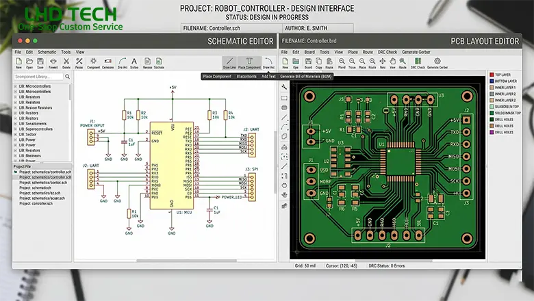
Step-by-Step: PCB Manufacturing Process
The manufacture of printed circuit boards is a multi-step process designed to turn a digital PCB design into a physical, production-ready electronic circuit board. Here’s how it typically works.
- It all starts with the PCB design and layout. Engineers use specialized software to lay out traces, vias, and pads based on the circuit schematic and performance requirements.
- Next comes material selection. You have to pick the right board material—FR4, ceramic, polyimide, or metal core—depending on what the application needs.
- Then there’s patterning. A layer of copper foil gets bonded to the insulating board. After that, a photo-imaging process defines where the copper should stay and where it needs to be removed.
- The next step is etching. Chemical etching takes away the unwanted copper, leaving behind just the conductive traces and pads.
- After etching, drilling happens. Mechanical or laser drills create holes for vias, through-hole component leads, and mounting points
- Once the holes are drilled, plating follows. Electroplating lines the inside of those holes with copper, which makes it possible to connect different layers of a multi-layer board.
- Then come the solder mask and silkscreen. The solder mask is applied and then cured. After that, the silkscreen is printed on top to add component reference labels.
- Surface finish is the next consideration. Finishes like ENIG, HASL, OSP, or immersion silver/gold are applied to protect the pads and improve solderability.
- Before any components go on, the bare board goes through electrical testing and quality assurance. Automated systems check for shorts, opens, and alignment issues.
- Once the board passes inspection, assembly begins. Components and connectors are soldered onto the board.
- Finally, there’s inspection and coating. Automated optical inspection (AOI) and X-ray checks verify quality. And if the board needs to survive harsh environments, a protective coating—acrylic, silicone, or parylene—may be applied.
PCB Design Tips for Reliability and Performance
The basics of PCB design go a long way toward ensuring a reliable, cost-effective, and easy-to-manufacture circuit. Here are important pcb design tips and best practices:
1. Match Board Material to Electronic Device Needs
- Choose substrate material for mechanical strength and electrical insulation to prevent warping and shorts.
- Always check that copper used in pcb matches the current-carrying and heat-sinking needs of your circuit.
2. Optimize Trace Width, Spacing, and Stack-Up
- The width and spacing of each trace and the proper stacking of copper and insulating boards ensure the PCB can handle current, noise, and signal speed.
- For power and high-speed digital circuits, controlled impedance in multi-layer boards is crucial.
3. Use Best Practices for Component Placement
- Place components like resistors, capacitors, and ICs to minimize routing complexity and maximize manufacturability.
- Ensure that connectors and key features are easily accessible for assembly and repair.
4. Design for Future Upgrades and Repairs
- Clearly label all components on the silkscreen.
- Make test points and essential components accessible from one side of the board whenever possible.
FAQs: What Printed Circuit Boards Are Made Of
Let’s bust some common myths and clarify critical details related to PCB manufacturing and use.
Q: What is the base material of a typical PCB?
A: Usually made from a combination of FR4 (fiberglass and epoxy) for rigid PCBs, polyimide for flexible circuits, or aluminum for metal-core boards.
Q: What types of materials like ceramics or advanced synthetics are used?
A: Ceramic materials (alumina, aluminum nitride) are used for high-frequency, high-thermal, or military boards; polyimide for wearables and flex circuits; advanced BT epoxy or cyanate esters for telecom/datacom.
Q: How do layers of copper help?
A: Multiple copper layers in a multi-layer PCB allow signal routing, EMI shielding, and separate power/ground planes—all crucial for advanced electronic devices.
Q: Can a board be made only of plastic?
A: No, because you need both insulating material for structure and copper (or other metals) for electrical conduction.
Q: What are typical defects if the wrong material is chosen?
A: Warping, electrical shorts, delamination, corrosion, overheating, and poor solder joint reliability—all can cause expensive failures.
Case Studies: How Printed Circuit Boards Are Used
1. Consumer Electronics: Smartphone PCB
A smartphone’s printed circuit board exemplifies the synergy of advanced pcb design and engineered materials. A 16-layer PCB in a flagship device is usually made of a combination of FR4 for general insulation and routing, polyimide in flex areas, and high-purity copper for all signal and power delivery. The board features:
- Rigid and rigid-flex circuit boards that allow for compact, stackable designs in slim phones.
- Layers of copper precisely arranged for signal integrity, data transfer, power regulation, and RF isolation.
- Components like passive elements (resistors, capacitors), integrated circuits, and antennas mounted to a PCB with automated assembly.
- Solder mask and specialized white or black silkscreen for crisp labeling and branding.
These boards and rigid assemblies must also dissipate heat from CPUs and charging circuits, requiring substrate material with both mechanical strength and electrical insulation.
2. Automotive Power and Lighting: Metal Core Printed Circuit
In the automotive industry, metal core printed circuit boards shine in lighting and power management. For example, an LED headlamp module’s board features:
- An aluminum or copper core base material to conduct and dissipate heat—a property crucial for long-lasting performance under high current load.
- Multi-layer boards with thicker copper used in pcb power layers to support dimming, CAN bus control, and diagnostics.
- Conformal or nano-coatings applied to ensure the pcb may survive moisture, salt spray, and thermal cycling in harsh environments.
Key features often include surface of the pcb intentionally exposed for direct heat transfer, integrated isolation slots for high voltage clearances, and dual-sided assembly for space savings.
3. Industrial and Medical: Rigid-Flex Circuit Boards
High-reliability fields like medical and industrial automation often use rigid-flex circuit boards.
- The board is made from a combination of polyimide for flexible zones and FR4 for rigidity.
- These circuits may be a single advanced pcb that allows for 3D installation, folding around corners or fitting precisely in custom housings.
- Components are mounted onto both the rigid and flexible areas to connect different electronic components and may feature gold-plated contacts exposed for connectors.
Materials like parylene conformal coating can add biocompatibility and chemical protection, making sure the printed circuit boards are made to last in demanding, life-saving applications.
Conclusion: Mastering PCB Materials and Design
In summary, the printed circuit board is the essential backbone of all modern electronics: a marvel of layered engineering, made of a combination of insulating materials, conductive copper, and protective coatings. Every PCB is designed with the interplay of substrate material, copper layer, solder mask, and more to guarantee that your electronic device works reliably, efficiently, and safely.
Key Reminders:
- PCB design always starts with material selection. Whether you need a rigid pcb for a desktop PC, a metal core printed circuit for a high-powered LED, or a flexible printed circuit for wearables, know your application and environment.
- Manufacture of printed circuit boards is a precision process—layers of copper and insulation come together to support every electronic component and connector.
- For every type of pcb, from single-sided boards to 16-layer boards with complex stackups, properties of each material dictate performance, durability, and manufacturability.
- Advanced boards often combine materials like ceramics, polyimide, metal cores, and various conformal coatings for extreme environments, medical devices, or the latest high-speed comms.
Whether designing the next smartphone or a rugged sensing system for autonomous vehicles, understanding what printed circuit boards are made of—and mastering PCB material science—will power your next innovation.