Understanding the PCB Lamination Process

In the world of electronic, the PCB lamination process stands out as a critical step in manufacturing printed circuit board. Lamination refer to the process that permanently bond the multiple layers of the PCB—including conductive copper traces and dielectric substrate material—into a single, unified circuit board. Without effective lamination, the pcb simply wouldn’t function or survive the stresses of its application.
Why Is Lamination Critical in PCB Manufacturing?

Proper pcb lamination determines:
- The mechanical strength of the printed circuit board.
- The reliability of signal transmission across circuit layer.
- The integrity of the dielectric insulation between copper plane.
- And ultimately, the PCB’s overall electrical performance.
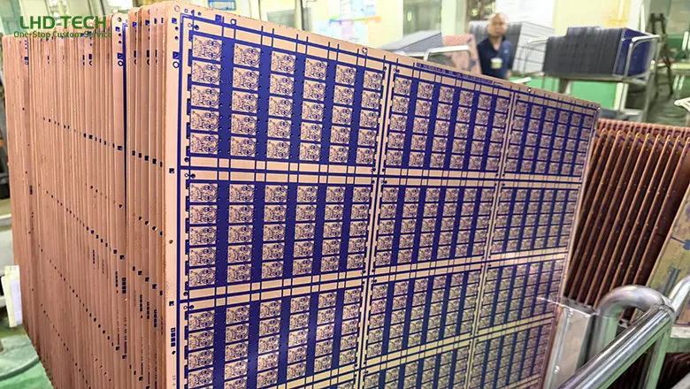
PCB fabrication always include this step: aligning the inner layers of the PCB, sandwiching them with prepreg or epoxy resin, then subjecting the stack to heat and pressure. This process involve special laminating presses, press plate, and alignment pin. Quality control at this stage is essential. It prevent problem like delamination and warping, which can compromise the functionality of the circuit.
Types of Lamination and Multilayer Lamination in PCB Fabrication

Lamination processes in the PCB industry have become increasingly diverse to support high-reliability application, fast prototyping, and mass manufacturing.
Cap Lamination vs. Foil Lamination
- Foil Lamination: In foil lamination, copper foil is applied on the outer layer of the stack before lamination. This is ideal for multilayer pcbs and allows easier etching for the outer circuit pattern.
- Cap Lamination: In cap lamination, a pre-etched core (with copper and dielectric) is surrounded by additional layer and laminated together. Cap lamination is common for circuit board with special requirement for thickness or controlled impedance.
Multilayer Lamination
Multilayer lamination is essential for advanced product in the PCB industry. Modern multilayer pcb manufacturing routinely build boards with 4, 8, 12, or more layer. These layer comprise:
- Alternating sheet of epoxy resin-impregnated prepreg.
- Copper sheet.
- And rigid core.
This technique enable embedding complex netlist and circuit within a single printed circuit board. After stacking, all layers are bonded together in a laminating press—a process critical in assembling PCB for high-speed and high-frequency application.
Understanding Sequential Lamination
When a board design require buried vias or complex HDI (high-density interconnect) feature, sequential lamination is used. This involve several successive lamination cycle, each adding layers or via structure. Sequential lamination ensures precise connection and support the most advanced PCB design approach, such as stacking blind vias and control impedance construction for signal integrity.
PCB Laminate Material Selection: Factors to Consider
Selecting appropriate laminate material is a foundational PCB design step and influences nearly every aspect of the pcb manufacturing process.
Key Factors to Consider
- Dielectric Constant: Lower constants (Dk) are favorable for high-frequency circuit.
- Epoxy Resin vs. Polyimide vs. PTFE:
- Epoxy resin (FR-4) is standard for most common pcb application.
- Polyimide offers better high-temperature stability—a must for aerospace and automotive circuit board.
- PTFE or Teflon is used for RF application, enabling outstanding signal transmission.
- Moisture Absorption & Flame Retardancy: Ensure environmental tolerance and safety.
- Glass Transition Temperature (Tg): High Tg reduce the risk of delamination during soldering and reflow.
- Coefficient of Thermal Expansion (CTE):Minimize CTE mismatch between layer prevent mechanical failure over time.
- Copper Thickness: Board can require thicker or thinner copper for power delivery, signal integrity, or fine-pitch routing.
Table: PCB Laminate Materials and Key Properties
| Material | Dielectric Constant | Tg (°C) | Moisture Absorption | Common Use Case |
| FR-4 | 4.2–4.7 | 135–180 | Low | Standard multilayer, most circuits |
| Polyimide | 4.1–4.4 | 200–250 | Very Low | Aerospace, high-temp, flex PCBs |
| PTFE/Teflon | 2.2–2.6 | 160–210 | Extremely Low | RF, microwave, high-speed pcb |
| CEM-1, 3 | 4.5–5.0 | <135 | Higher | Low-cost consumer circuits |
Tips for PCB Designers
- Always match substrate and copper layer properties with your circuitry’s requirement.
- Work closely with supplier to verify that selected material support your board’s intended lamination processes.
- Simulate stack-ups using PCB design software and confirm with a material engineer during early design review.
Step-by-Step Process: How PCB Lamination Works

The PCB lamination process is both an art and a science. Let’s walk through a modern step-by-step process for manufacturing printed circuit board:
Preparation of Inner Layers
- Inspect and clean each copper layer.
- Apply micro-etch or black oxide treatment for maximum adhesion.
- Pre-align the inner layers of the PCB using alignment pins and automated registration system.
Layer Stack-Up
- Alternate inner copper circuit and dielectric prepreg, stacking according to the planned PCB design.
- Add outer layer—either copper foil for foil lamination, or laminated sub-assemblies for cap lamination.
- Insert press plate as needed to maintain flatness in the laminating press.
Heat and Pressure Cycle
- Place stacked layer in a heated hydraulic or vacuum laminating press.
- Apply high temperature and pressure (typ. 170–210°C, 200–400 psi) to melt the resin in the prepreg, forcing it to fill all voids and surround copper feature.
- This stage is the literal bonding point: the resin flows around conductor, expelling air, and fully forms the printed circuit.
Cooling and Releasing
- Gradually cool the stack under pressure to stabilize the laminate and prevent warpage or stress inside the circuit board.
- Eject and remove press plate.
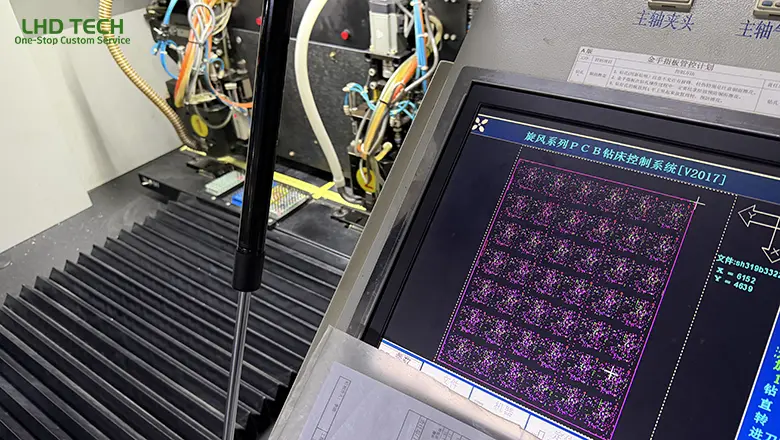
Drilling and Plating
- Drill holes for through vias, blind vias, and component mounting.
- Use laser drills for smaller, more precise via structures in HDI boards.
- Following lamination, the circuit board is sent for plating (copper deposition), forming electrical connections between layer.
Final Steps
- Pattern outer copper layers with photolithography and etching.
- Solder mask application and legend printing.
- Comprehensive inspection, electrical test, and QA.
Sequential Lamination: Advanced Lamination Processes for Complex Circuits
Sequential lamination is indispensable in pcb manufacturing where designs are too complex for traditional single-stage multilayer lamination. By carefully bonding new layers onto existing laminated circuit, sequential lamination gives engineer the power to produce incredibly dense, reliable, high-speed circuit assembly.
How Sequential Lamination Enhances PCB Fabrication
- Support Blind and Buried Vias: By building up the layer stepwise and performing interlayer drilling and plating operations between lamination stage, sophisticated via structure can be realized—enabling next-generation signal routing in space-constrained device.
- Promotes Signal Integrity: Sequential lamination allow for precise placement of ground and power plane close to signal layer, minimizing impedance mismatch and electromagnetic interference.
- Facilitates HDI (High-Density Interconnect) Circuits: Smartphone, wearable, and high-speed router depend on these advanced lamination processes to connect fine-pitch BGA and advanced IC.
The Sequential Lamination Process (Step-by-Step)
- Initial Stack-Up and First Lamination Stage:
- The core of the board—including several copper and dielectric layers—is laminated using standard procedures.
- Drill and Plate:
- Drill holes for vias that need to connect current layers. Plate these holes with copper, linking the relevant layers.
- Additional Layers Added:
- Stack extra prepreg and copper layers atop the initial assembly.
- Insert alignment pins or use optical/X-ray alignment for perfect registration.
- Repeat Lamination:
- Apply heat and pressure to bond the new layers, ensuring resin in the prepreg fills all voids and forms strong, reliable bonds.
- Drilling and Plating as Needed:
- Further drilling and plating can occur at each stage to continue adding complexity.
- Final Steps:
- Once all layers are stacked and bonded, perform final drilling and plating, outer copper etching, solder mask, and comprehensive PCB QA testing.
Drilling and Plating in PCB Manufacturing Process
Drilling and plating are the linchpins that translate a multilayer laminate into a functional printed circuit board. Following lamination, these processes establish the vertical electrical connection (vias) vital for modern electronic.
Drilling: The Gateway for Inter-Layer Connections
- Mechanical Drilling: Using for standard through-holes and larger via structures.
- Laser Drilling: Essential for micro vias (often <0.2mm in diameter) used in HDI, sequential lamination and blind via
- Registration: Alignment pins or X-ray registration ensure that drilled hole precisely hit the copper pad on each layer in the stack.
Plating Processes
- Electroless Copper Plating: Deposit a thin copper layer on via wall, providing electrical connectivity between layer.
- Electroplating: Builds up the copper thickness in the vias and sometimes on the outer layer for added conductivity and reliability.
Best Practices for Drilling and Plating
- Always check for smear-free holes after drilling; contamination can cause via failure after assembly.
- Use advanced pcb design software to optimize drill files and plating logic for the complexity of the design.
- Perform solder float tests and microsection analysis to verify plating quality.
| Process Step | Purpose | Performance Checks |
| Drilling | Open paths for vias/components | Hole wall roughness, registration |
| Plating | Electrical interconnects | Adhesion, cross-section uniformity, cracks |
| Final Cleaning | Remove residues before assembly | Surface inspection, ionic purity tests |
Challenges, Solutions, and Common PCB Lamination Issues
Every lamination process faces risks. However, knowing the most common PCB problems—and their solutions—ensures consistently high yield.
Common PCB Lamination Issues
- Delamination: Often due to insufficient resin cure, high moisture in layers, or excessive pressure/temperature gradients. Solution: Controlled curing, pre-baking prepreg/core, and precise process monitoring.
- Voiding/Bubbles: Trapped air or gas leads to open circuits or weak interlayer bonds in the final PCB. Solution: Use of vacuum presses, slow and uniform heat ramping, and material out-gassing protocols.
- Misaligned Layers: Poor registration can render sections of the circuit open or shorted. Solution: Use advanced alignment systems (optical/X-ray) and constantly calibrate alignment pins.
- Warping/Mechanical Stress: Asymmetrical stack-ups or rapid cooling can cause bowing of the finished circuit board. Solution: Design symmetrical stack-ups and adopt gradual cooling practices after lamination.
Tips for Robust Lamination
- Never skip material pre-conditioning; moisture destroys lamination reliability.
- Use high-Tg laminate materials in demanding, high-temp, or lead-free assembly environments.
- Routinely verify resin flow in the prepreg and control all lamination press cycle parameters with SPC (statistical process control).
Best Practices and Tips for Effective PCB Lamination and PCB Design
Modern pcb fabrication merges science, automation, and human expertise. These best practices cover the process from PCB design on screen to a successful, durable hardware product.
Tips for PCB Designers
- Use stack-up simulation tools during the pcb design process to anticipate thermal/CTE behavior and impedance across layers.
- Specify outer copper weights and laminate material types directly in your design files.
- Choose via structures that match your manufacturer’s lamination processes—especially for HDI designs with blind/buried vias.
Tips for Manufacturers
- Store all materials in controlled environments; humidity and heat can ruin epoxy resin before use.
- Routinely inspect alignment pins, press platens, and lamination cycle logs for wear or drift.
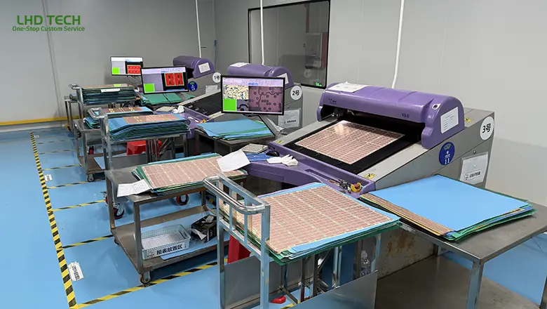
- Inspect both raw and finished boards with AOI (automated optical inspection) and microsectioning.
Case Studies and Real-World Examples from the PCB Industry
Case Study 1: Telecommunication—Signal Integrity in High-Layer PCBs
A major telecom OEM require a 16-layer HDI board with tight impedance control for 56-Gbps SerDes channel. Their fabricator used seven sequential lamination step, with vacuum press cycles for each, and performed Scanning Acoustic Microscopy (SAM) after every stage. The result was flawless signal performance with zero delamination—a must for network reliability.
Case Study 2: Medical Device—Reliability in Harsh Environment
A biomedical company redesign its imaging circuitry using PTFE-based laminate and polyimide layer. After introducing slow ramp-up/cool-down cycles and switching to immersion silver for outer copper plating, PCB durability improved, and failure in the field dropped by 90%.
Frequently Asked Questions: PCB Lamination and Multilayer PCB Manufacturing
Q: What differentiates foil lamination and cap lamination in PCB fabrication?
A: Foil lamination builds outer layers using copper foil and prepreg; cap lamination uses laminated cores with additional layers applied. Foil is common for standard multilayers, while cap is used for high-precision, impedance-controlled circuits.
Q: Is sequential lamination required for all multilayer PCBs?
A: No. Most standard multilayer designs use a single lamination stage. Sequential lamination is essential only when the design requires buried or staggered blind vias.
Q: How is registration between layers ensured during the lamination stage?
A: Manufacturers employ alignment pins, optical targets, or X-ray registration during stack-up. These methods guarantee each drilled via will meet its intended copper pad in the finished circuit board.
Q: How does the choice of laminate material affect PCB design and fabrication?
A: Key properties like Tg, CTE, dielectric constant, and moisture absorption influence the process window, performance, and long-term reliability of the PCB. Always match material properties with the board’s service environment and circuit speed.
Q: What is the role of drilling and plating after lamination?
A: Drilling opens up the layers for vertical connections or components; plating covers the hole walls with conductive copper, creating critical inter-layer electrical paths.
Conclusion: Mastering the Lamination Stage in Modern PCB Fabrication
Lamination is the essential bridge between PCB design and robust, real-world hardware. By understanding and controlling every parameter of lamination processes—from selecting the right laminate materials, controlling resin flow and alignment, to managing complex via structures with sequential lamination—designers and manufacturers ensure durable, reliable, and high-performance printed circuit boards.
Key Elements of a Reliable PCB Lamination Process
| Element | Importance | Best Practice |
| Material Selection | Signal/control, cost, reliability | Confirm Tg, CTE, Dk, Df, and resin compatibility |
| Stack-Up Design | Performance, manufacturability | Use DFM, simulate with PCB design software |
| Lamination Process | Physical integrity of the circuit | Precise temperature and pressure control, moisture management, calibrated laminating press |
| Drilling & Plating | Reliable connectivity between layers | Employ laser/precision drills, regular tool calibration, optimized plating chemistry |
| Inspection & Testing | Prevents latent failures, yield impact | Employ AOI, X-ray, microsection, IST, SAM, and peel testing |
The lamination stage is much more than just pressing layers together—it is a sophisticated science that balances material science, advanced machinery, and deep industry experience. Whether you are building simple prototypes or high-reliability, mission-critical circuit boards, following best practices at every step of the PCB lamination process pays dividends in performance, durability, and ease of manufacturing.
The Future of Lamination and PCB Fabrication
PCB fabrication trends are moving towards higher speeds, thinner dielectrics, more sequential lamination cycles, and reliance on data-driven quality control. Manufacturers are innovating with lower-CTE substrates, ultra-low Dk laminates for mm Wave/RF applications, and enhanced automation in alignment, drilling, and lamination stages.
Sustainability is also growing in importance: Future lamination processes may incorporate greener resins, lower-emission press cycles, and recyclable materials, in response to both regulation and industry-driven environmental responsibility.
Final Thoughts and Call to Action
Whether you are designing your first PCB or bringing the next innovation to market, mastery of the lamination stage is key to turning great designs into reliable products. Every pcb design choice, from laminate material to stack-up technique, impacts manufacturability, yield, cost, and long-term function.
If you have challenges with lamination processes, sequential lamination, or multilayer fabrication, don’t hesitate to contact our team for a consultation or project review. For more technical deep-dives, subscribe to our blog or check out our resources above.