
Introduction

When talking about bare PCBs—the foundation of every electronics assembly—we’re referring to boards that have completed manufacturing steps but haven’t yet had electronic components mounted onto the board. The bare board provides all electrical pathways needed for assembly but is sometimes overlooked in the excitement of working with a fully functional PCB.
A thorough understanding of bare PCB boards is fundamental knowledge that professionals engaged in PCB design, manufacturing and testing must possess. In the initial stages of PCB manufacturing, the core objective is to ensure that bare boards achieve high reliability and defect-free quality. Such high-quality bare boards form the foundational support for constructing various complex, high-density integrated printed circuit boards, with their applications spanning multiple critical fields, including smartphones, industrial automation equipment and medical instruments. Conducting comprehensive testing of bare boards serves a dual purpose: on one hand, it ensures that the circuit board fully meets design specifications before assembly, and on the other hand, it enables the early identification and elimination of any potential defects that could cause damage to the board itself or subsequent integrated equipment.
Let’s explore the nuances, advantages and production process for bare PCBs, the key stages of board development and why bare board testing matters for quality, reliability and the electronics revolution itself.
Defining Bare, Blank, and Zero PCBs
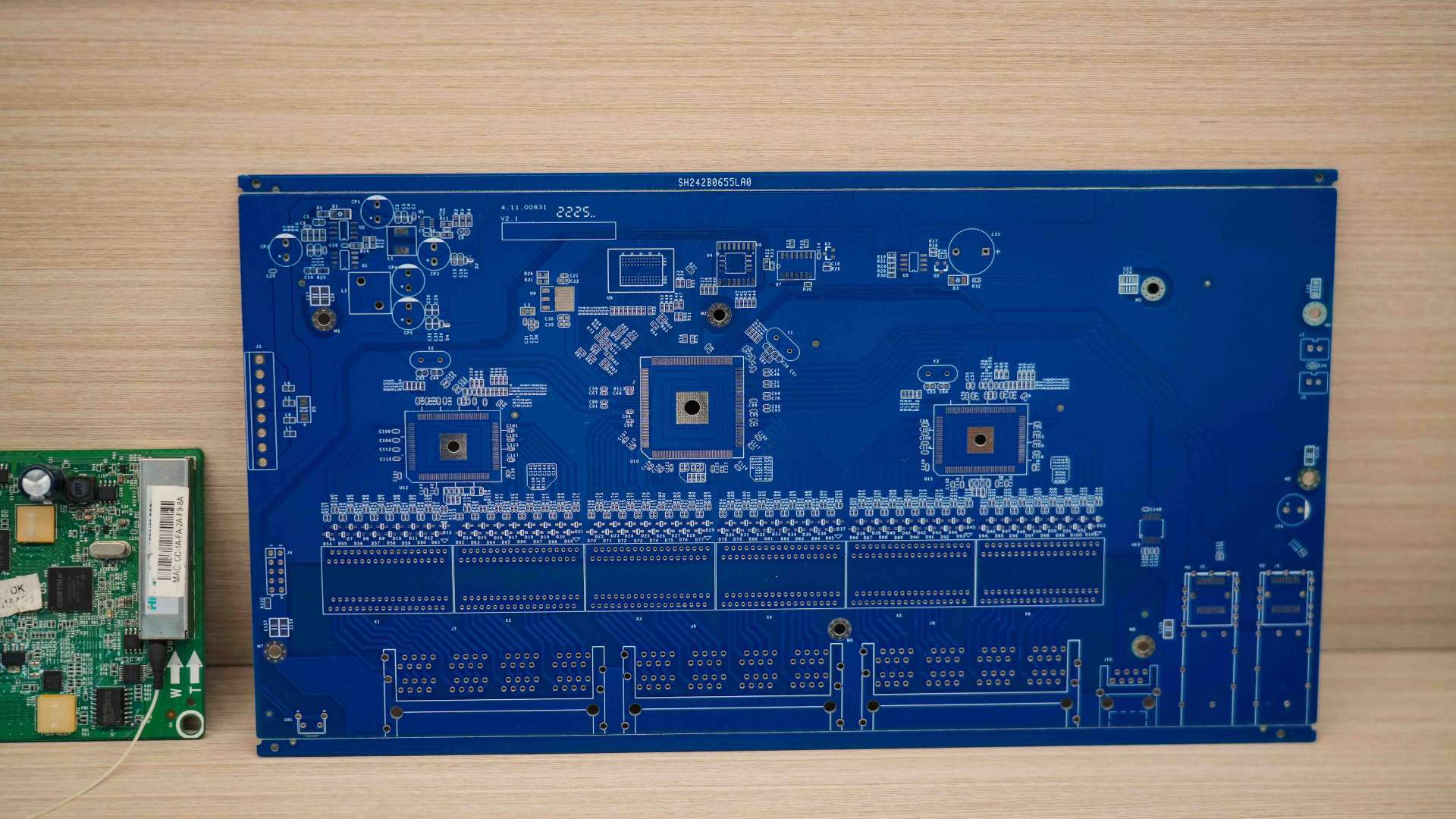
A bare PCB (bare printed circuit board) is a complete circuit board without any electronic components soldered in place. This unpopulated circuit board (also known as a blank or bare PCB) is ready for component placement and assembly, typically provided with copper traces, pads, vias, solder mask and silkscreen.
Bare PCB Board in Context
A bare PCB board isn’t a “blank board” in the sense of a plain sheet; it’s manufactured with the specific circuitry designed in software. The board refers to the actual fabricated substrate and copper layers representing a ready-to-populate platform.
What’s a Zero PCB?
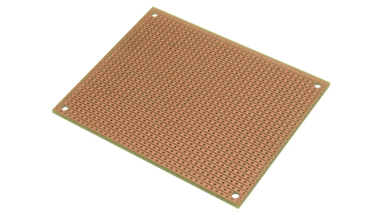
A zero PCB is a term called zero PCB or perfboard, also known as perfboard or DOT PCB. This generic board features a grid of electrically isolated pads—there are no designed traces across the PCB, providing maximum flexibility for custom circuit creation. Zero PCBs are ideal for rapid experimentation and educational environments.
Comparison of Bare, Blank, and Zero PCB Boards
| Type | Definition / Use | Features | Applications |
| Bare PCB Board | Board without components, includes traces & mask | Board layout, mask, silk | PCB manufacturing, PCBA, QC |
| Blank PCB | Plain copper-clad, no traces, holes, or silk | Pure substrate, copper | Custom etching, prototyping, R&D |
| Zero PCB | Grid-style, unconnected pads, generic board | Called perfboard or DOT | DIY, educational, fast prototyping |
Structure of a Bare PCB Board

A bare circuit board is built for maximum function and reliability. It may look simple, but the bare PCB includes highly engineered layers:
Layers of the PCB
- PCB Substrate (Base Material): The backbone for the board, typically made from FR-4 (fiberglass epoxy) or flexible polyimide. Some power applications use aluminum or ceramic for enhanced thermal performance.
- Copper Traces: Thin copper lines on board surfaces and inside layers act as “wires,” connecting pads and vias into a complete circuit board.
- Solder Mask: The solder mask is a green or other colored polymer protective coating applied to the surface of a PCB. This coating effectively prevents the formation of solder bridges during the soldering process, provides oxidation protection for copper traces and enhances the overall reliability of the bare board in subsequent assembly and usage through electrical insulation.
- Silkscreen: The silk screen layer is a marking layer printed on the surface of the circuit board using white or colored ink. These markings are used to indicate component reference designators, display polarity orientation, print company logos and provide practical guidance for assembly operations.
- Pads and Vias: Exposed copper areas for soldering and metalized holes for multi-layer connection, forming the backbone of reliable bare PCBs.
- Surface Finish: Protects copper and ensures solderability—common types are HASL and ENIG.
A board without components is much easier to inspect. Any error found at the bare board stage is simpler, cheaper and less destructive to the board overall.
Bare PCB Manufacturing Process: From Design to Reality

The bare PCB manufacturing process starts with digital PCB design software—here, you create the board layout, define netlists, and specify all copper layers, silkscreen and mask details.
Stages of Board Development
- PCB Design in Software:Using CAD tools (like Altium Designer), the complete circuit board is mapped out in virtual layers.
- File Preparation:Output Gerber files and a drill file.
- Fabrication Process:
- Laminating the Substrate:Formation of the PCB substrate.
- Copper Application and Imaging:Using photolithography, your design is printed.
- Etching:Unwanted copper is removed, leaving only the traces.
- Drilling and Plating Vias:Automated machines create precise connections.
- Solder Mask and Silkscreen Printing:Protect and guide assembly.
- Surface Finishing:Ensures the interface remains solderable.
- Bare Board Testing:Before any electronic components touch the bare printed circuit board, it must be electrically tested.
PCB manufacturing is a blend of precision, speed and innovation. Top-tier PCB manufacturers now provide online design verification and offer DFM (Design For Manufacturability) checks to minimize errors in the early stages of PCB manufacturing.
Types of Bare Board Testing

Bare board testing is an electrical test executed on a bare PCB before assembly. The goal: ensure the board matches the design, is free of shorts/opens and can become a reliable, fully functional PCB after population.
Core Types of Bare Board Testing
- Flying Probe Test:Automated probes scan the board, contacting test points and pads as dictated by the netlist. Very flexible, ideal for prototypes, rapid changes and smaller production runs.
- Fixture Test (Bed-of-Nails/In-circuit Testing):A custom fixture with spring-loaded pins contacts hundreds (even thousands) of points simultaneously. This is suitable for large-scale manufacturing and ensures consistent, repeatable results.
Additional Methods
- AOI (Automatic Optical Inspection):High-resolution cameras find mask misalignments, broken traces or soldering issues, often before or after electrical test.
- X-ray Inspection:Critical for multilayer PCB boards, revealing hidden defects without being destructive to the board.
Benefits of Bare Board Testing
- Detects Issues Early:Saves money by catching errors before assembly.
- Ensures Batch Consistency:Especially when PCBs are often densely populated.
- Supports High-Reliability Markets:Such as aerospace and medical electronics, where quality assurance is paramount.
Types of Bare Board Testing—Advantages and Where to Use
| Type | Best For | Advantages |
| Flying Probe Test | Prototypes, small/medium batches | Fast setup, no fixture needed |
| Fixture Test | Mass production | Consistent, fast, economical at scale |
| AOI | All production runs | Non-contact, fast defect detection |
| X-ray Inspection | Multilayer and HDI boards | Non-destructive for hidden layer faults |
Benefits and Applications of Bare Boards in Engineering
Bare PCBs play an essential role in every branch of electronics engineering. Before a pcb board becomes a fully assembled product, the bare board provides a sturdy, reliable canvas for all subsequent production and testing steps.
Advantages of Bare Board in Production and R&D
- Early Detection of PCB Layout Issues Testing bare boards ensures that the board layout matches the design files. Any deviation—like open or short circuits—can be addressed before it becomes destructive to the board or leads to costly scrap later in PCB assembly.
- Quality Control and Assurance Bare board testing becomes critical for medical, aerospace, and automotive industries, where high-reliability bare PCBs are non-negotiable. Using bare board testing in these fields builds confidence that the base platform is impeccable.
- Cost Savings in Scale Detecting errors in bare PCB boards during the early stages of PCB manufacturing greatly reduces losses, especially when boards are produced in the thousands. The cost of repairing or remanufacturing a complete circuit board populated with expensive electronic components is far higher than fixing a bare board.
- Optimal Design Verification Engineers can use bare boards for direct soldering, motor-driving prototypes or running pre-assembly functionality tests. This stage is suitable for large-scale manufacturing because it standardizes quality and speeds the PCB fabrication process.
- Flexibility for Iterative Design Since bare printed circuit boards are unpopulated, any necessary last-minute design tweaks can be more readily implemented compared to fixing errors post-PCBA.
Applications of Bare Boards
Bare circuit boards are foundational in nearly every electronics sector:
- Consumer Devices:Phones, tablets, wearables and smart home equipment all start as bare PCBs.
- Automotive Controls:Engine controllers, infotainment units, and advanced sensors.
- Industry & Power:PLCs, motor drivers, LED lighting (especially with metal core PCBs).
- Medical Electronics:Diagnostic equipment, therapy systems and monitoring platforms.
- Aerospace & Defense:Reliable bare PCB boards are indispensable in flight systems and secure communications.
- IoT and Smart Sensors:Both rigid and flexible bare PCBs provide the backbone for distributed smart systems.
Real-World Applications of Bare Boards in Engineering
| Sector | Typical Bare PCB Used | Reliability Feature |
| Automotive | Multilayer PCB, metal core | Thermal resistance, vibration proof |
| Medical | Rigid-flex, controlled impedance | EMI shielding, long-term durability |
| Consumer Electronics | FR-4, high-density board | Space-saving, mass production ready |
| Industrial | Blank or bare, heavy-copper | Load capacity, power handling |
Bare PCB vs. Assembled Board and Zero PCB

Bare PCB vs. Assembled Board (PCBA)
A bare PCB board is a board without components. The next stage in the electronics process is the assembled board (PCBA), where all electronic components are placed and soldered, making the board fully functional.
Benefits of Using Bare Board Testing Before Assembly
- Protects Components:By ensuring no open or short circuits exist before population, bare board testing protects sensitive ICs and other valuable parts.
- Guarantees Fully Functional PCB:When you assemble onto a verified bare printed circuit board, the result is a reliable product ready for end use.
- Improves Yields:Especially in high-volume manufacturing, early detection means higher yields and fewer returns from faulty complete boards.
Bare PCB vs. Zero PCB
Bare PCB Board:
- Custom manufactured to specific design—used in modern electronics production and suitable for large-scale manufacturing.
- Includes mask, silkscreen, vias, surface finish and supports multi-layer stackups.
Zero PCB (Perfboard/DOT PCB):
- A generic board, ideal for quickly building test circuits or educational projects.
- Features a grid of pads with no predefined traces (hence the term board without traces)—also known as blank or bare, but truly meant for DIY custom wiring and not scalable or suitable for commercial manufacturing.
How to Order a Reliable Bare PCB Board
Steps to Procure a High-Quality Bare Board
- Finalize Your PCB Design Use PCB design software such as Altium Designer, KiCad, or Eagle. Ensure your board layout and netlist files are error-free.
- Prepare All Design Files This includes Gerber files for each copper layer, solder mask and silkscreen, and a drill file for vias and holes. Always follow the specs listed by your PCB manufacturer.
- Select the Right PCB Manufacturer Look for vendors experienced in your specific vertical—medical, automotive, high-frequency communications, etc. Good manufacturers provide DFM checks, online quotes and support multi-layer PCB and detailed surface finishes.
- Choose Board SpecificationsLayer count (single, double or multilayer PCB)
Base substrate (FR-4, polyimide, metal core)
Copper thickness
Surface finish (ENIG, HASL)
Solder mask color and silkscreen
- Review Bare Board Testing Options Decide between flying probe or fixture-based tests. For high-reliability applications (like critical sensors or mission equipment), request a certificate of bare PCB testing with your shipment.
- Order and Inspect Upon Arrival Look for well-defined traces, even mask coverage, no surface scratches and properly plated holes. Spot-check with a multimeter for continuity across the board.
Tips for Handling, Storing and Testing Bare Printed Circuit Boards
Bare PCBs need careful handling to remain reliable and solder-friendly for assembly:
- Handle by Edges:Minimize direct touch on copper surfaces of the pcb board.
- ESD Precautions:Use anti-static mats and wristbands—board without protection can accumulate static, degrading future performance.
- Clean, Dry Storage:Store in sealed anti-static or moisture barrier bags. Desiccant packs help absorb humidity, which can damage solderability over time.
- FIFO Inventory:Use “first-in, first-out” shelf management, especially with ENIG or OSP-finished boards.
- Post-Testing Storage:After bare board testing, mark tested boards with a sticker or QR; this helps with traceability (an essential part of modern electronics supply chains).
Best Practices for Reliable Bare PCB Handling
| Tip | Why It Matters |
| Use bare boards with gloves | Prevents oils or corrosion on pad/traces |
| Avoid stacking surfaces on the pcb board | Prevents abrasion, maintains mask and silk integrity |
| Store away from UV light | Protects sensitive solder mask/ink |
| Track revisions and lots | Helps identify root-cause if failures emerge downstream |
PCB Design Guidelines and Layer Considerations
Early Stages of PCB Manufacturing Begin with Smart Design
- Layer Planning:More layers mean better routing and shielding, but also higher cost and complexity.
- Impedance Control:Use bare pcb with careful trace and via design to maintain impedance for fast, high-frequency signals—critical for RF, USB, HDMI and similar applications.
- Board Layout for Manufacturability:Rounded corners, consistent pad sizes and proper pad-to-hole ratio all ensure easy assembly and reduce mechanical stress.
Frequently Asked Questions: Bare Boards & PCB Testing
Q: Does every board require bare board testing before assembly?
A: Yes, for any project where reliability and long-term performance matter. Bare board testing ensures every layer and pathway is as intended, preventing faults that could render a thoroughly populated pcb board useless.
Q: How many layers can a bare PCB have?
A: From a simple single-sided pcb board to complex multi-layer PCB configurations (10 layers or more). Applications of bare boards in engineering increasingly lean toward high-layer counts for compact, high-speed electronics.
Q: Is bare PCB testing destructive to the board?
A: Not at all. Bare PCB testing is non-destructive and designed to preserve the integrity of the unpopulated circuit board for subsequent assembly.
Q: Can I specify a mixture of surface finishes or solder mask colors?
A: Yes. For special applications (like LED lighting), mixing finishes can optimize both performance and aesthetics.
Q: Does a zero PCB support large-scale manufacturing?
A: No. Zero PCBs (perfboards) are for prototyping and not suitable for commercial, scalable production or for products with stringent certification requirements.
Conclusion: The Role of Bare Boards in Electronics
The bare PCB board is where the journey of every electronic device truly begins. By embracing the advantages of bare board testing, electronics engineers and manufacturers can deliver more reliable, scalable and innovative products. From the earliest stages of board development to the final testing of an assembled and fully functional PCB, the reliability and quality of your bare board sets the tone for every downstream process.
Applications of bare boards in engineering range from household gadgets and industry controllers to cutting-edge medical and communication systems. As standards rise and complexity increases—particularly with multilayer PCB demands and rapid prototyping—investing in reliable bare PCBs, robust manufacturing and rigorous bare PCB testing is essential.
Bare boards play a foundational role in electronics. Their design, manufacturing and verification ensure that the final complete circuit board (and the products it powers) meet the demanding expectations of contemporary technology. Choose a suitable PCB manufacturer, collaborate closely during design, and always use bare board testing as your quality gate before assembly.


