Introduction: Understanding HDI PCBs and High Density Interconnect Technology
The rapid development of the electronics industry is driven by the ongoing trend of miniaturization, continuous performance enhancement, and the capacity to reliably integrate more components within increasingly compact spaces. High-Density Interconnect (HDI) printed circuit board technology stands at the core of these advancements, achieving wiring densities beyond previous imagination.
What is an HDI PCB?
HDI PCBs represent a specialized category of printed circuit boards.By adopting fine traces, tight spacing and advanced interconnection technologies, they can accommodate a greater number of components within a smaller form factor.Engineers can leverage this technology to integrate complex circuits.End products enabled by HDI technology are lighter, thinner, more efficient in operation and more reliable in performance than those based on traditional PCBs.
Why Are HDI Boards Essential?
The electronics industry relies on PCBs with higher wiring density, especially for wearable devices, IoT, advanced medical equipment and next-generation telecommunications. Understanding HDI and leveraging advanced circuit boards is now a must for engineers aiming for market-leading products.
This guide is structured around HDI PCB manufacturing. It covers PCB design principles and cost comparisons. It also covers circuit board characteristics and future trends in high-density interconnect technology.
What Are HDI PCBs? Core Concepts in High Density Interconnect

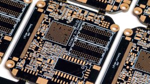
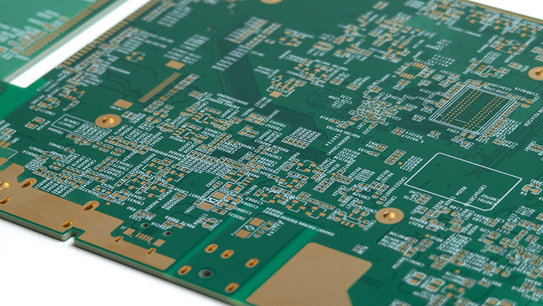
HDI boards—high density interconnect solutions are a major leap forward in printed circuit board (PCB) technology. At their core, these advanced circuit boards are engineered for maximum density per unit area compared to traditional circuit boards.
What Makes HDI Boards Different?
- Smaller Vias and Microvia Technology: HDI PCBs are characterized by microvias. These microvias are formed using laser drilling technology, with diameters typically less than 150 microns. This feature enables denser vertical interconnections between different layers of the PCB.
- Blind and Buried Vias: Only connect necessary layers, maximizing routing options and preserving space that would be lost with through-hole vias.
- Fine Pitch and Narrow Traces: The manufacturing techniques used for HDI PCBs support much narrower traces and smaller spacing, compared to standard PCBs.
- Sequential Lamination Process: The multilayer PCB stackup is built up in stages, allowing each layer to be interconnected with the smallest possible vias.
HDI PCB vs. Standard PCB
| Feature/Attribute | Standard PCB | HDI PCB / High Density Interconnect |
| Via Type | Plated Through-Hole | Microvias, Blind, Buried |
| Trace Width | 100–250μm | 40–75μm |
| Layers | 2–8 (typical) | 8–24+ (compact form) |
| Wiring Density | Moderate | Boards with higher wiring density |
| Interconnection | All layers (limited options) | Advanced interconnect, many options |
| Component Density | Moderate | Greater number of components |
Key Features of HDI Boards—High Density Interconnect Advantages

High density interconnect boards are distinguished by several advanced features that enable them to outperform traditional circuit boards, especially for compact or high-speed designs.
1. Microvias, Blind Vias and Buried Vias
- Microvias use laser drilling technology for minuscule via creation, allowing tighter routing and high density per square cm than any mechanically drilled board. This is the heart of HDI PCB manufacturing.
- Blind vias connect the surface to one or more internal layers, while buried vias connect only inner layers—both maximizing layer usage and circuit compactness.
2. Finer Lines and Spaces
- PCB manufacturing for HDI boards enables thinner traces and higher wiring density, necessary for devices requiring a compact form without sacrificing performance.
3. Advanced PCB Materials and Lamination Process
- The lamination process for HDI involves stacking different layers of the PCB and fusing them using advanced materials designed for thermal management and electrical insulation—supporting improved performance at high frequencies.
4. Sequential Build-Up Process
- Sequential lamination lets engineers stack and interconnect as many as 20+ layers, a process especially beneficial for multilayer PCB.
- Enables embedding shielding, power and even passive components within the board architecture.
5. High Density Layouts and Advanced Design Software
- Professional PCB design software underpins the development of high-density interconnect (HDI) boards.It is capable of managing the complexity involved in HDI layout Design teams rely on these tools to overcome technical challenges throughout the layout process,while successful manufacturing also depends on the design robustness enabled by such software.
The Process of HDI – Key Steps in HDI PCB Manufacturing

The HDI manufacturing process involves several unique steps that differentiate it from standard PCB manufacturing techniques.
1. Advanced Layer-by-Layer Stackup and Lamination Process
- Layers are constructed using sequential lamination, with each new layer increasing the total wiring and routing density.
- The result is a circuit board with higher wiring density and a greater number of signal and power paths within a smaller physical space.
2. Microvia and Laser Drilling Technology
- The laser drilling process undertakes the task of creating microvias. Microvias are fundamental structures for achieving high-density interconnections. Both CO2 laser equipment and UV laser equipment can be used for this process. These devices machine precise microvia structures onto the circuit board. Microvias provide a physical pathway for advanced vertical interconnections. Signal loss during transmission is also minimized through this design.
- Microvia technology supports blind via, buried via and stacked via combinations for the most complex HDI designs.
3. Copper Plating: Electroless and Electrolytic
- A thin copper layer is deposited within microvias using electroless plating, followed by electrolytic plating to build up the conductive path, improving reliability for high density signal routing.
4. Imaging, Etching and Solder Mask Application
- High-resolution imaging and etching techniques support the creation of extremely fine lines and pads.
- Solder mask is applied for material properties like insulation and protection, a crucial factor given the compact form and fine features in HDI PCBs.
5. Automated Optical Inspection and Testing
- Advanced AOI and in-circuit testing verify the integrity of each microvia and trace—essential as defects are harder to detect and repair in high density boards.
HDI vs Traditional PCBs: How High Density PCBs Compare
1. Circuit Density and Board Size
HDI boards—high density interconnect are vastly superior in circuit density, supporting a much greater number of components in a smaller board area compared to standard PCBs.
2. Electrical Performance
HDI technology supports improved performance by reducing signal path lengths, lowering resistance and inductance between different layers, and minimizing the risk of signal integrity problems like EMI and crosstalk. The use of microvias and smaller vias through laser drilling allows circuit designers to optimize routing for high-speed, high-frequency signals, resulting in a clear reduction in signal loss compared to traditional PCBs.
3. Multi-layer Possibilities and Compact Form
HDI PCB manufacturing technology supports the design of complex multilayer boards. These multilayer boards can have a layer count ranging from 10 to 16 or even 24 layers. Their overall form factor is typically much smaller than that of traditional circuit boards. The sequential lamination process, buried via technology, and advanced materials provide designers with flexibility. Designers can precisely position power layers, ground layers and signal layers where they are needed.
4. Comparing Manufacturing Process
| Aspect | Traditional PCB | HDI Board / High Density Interconnect |
| Drilling Method | Mechanical | Laser drilling/laser via formation |
| Component Density | Moderate | High density per unit area |
| Layer Additions | Single Lamination | Sequential build-up/lamination process |
| Via Type | Full through-hole | Microvias, blind/buried vias |
| Typical Applications | Basic consumer electronics, industrial control | Smartphones, tablets, medical, telecom, automotive, aerospace |
| Board Size | Larger, less compact | Compact form, minimalist footprint |
| Signal Integrity | Good for low-speed | Supports high-speed digital signals |
| Flex/rigid-flex Integration | Limited | Well-supported by HDI designs |
5. Design Flexibility
HDI design differs from traditional PCBs. HDI design supports the integration of fine-pitch BGAs, high-pin-count ASICs and advanced microcontroller units. In applications with stringent requirements for board size, weight or advanced packaging, HDI design enables the embedding of more advanced functions. This technology also supports multi-layer stacking and aims to maximize the utilization of every square millimeter of space.
Benefits of HDI Technology in PCB Manufacturing

HDI technology possesses various significant advantages. These advantages make it a critical process in the manufacturing of next-generation electronic products.
1. Benefits of HDI: Miniaturization, High Performance and More
- Greater Number of Components into a Smaller Space: The ability to integrate high-performance electronic devices into the smallest possible space constitutes a competitive advantage. This advantage is particularly evident in the fields of smartphones, fitness trackers and IoT sensors.
- Improved Performance and Reduced Signal Loss: Enhanced signal integrity is a key advantage of HDI boards. Microvia technology and short, direct high-density interconnect routes enable this advantage.
- Lower EMC/EMI: HDI circuit boards employ denser ground planes and rational routing. This design not only effectively reduces spurious emissions but also enhances immunity to interference.
- Built for High-Speed Design: HDI PCB manufacturing technology supports the handling of GHz-level signals through advanced impedance control.
- Layer Optimization and Thermal Management: HDI circuit boards utilize different layers to set up dedicated structures. These structures include power planes, ground planes or embedded heat sinks. This results in improved heat dissipation.
- Material Properties: Advanced materials selected during HDI PCB manufacturing (such as high Tg FR-4 or polyimide) provide superior performance in demanding temperature and frequency ranges.
2. Application Examples
- Medical Electronics: HDI technology enables the manufacturing of smaller, lighter implantable devices. It also supports the manufacturing of advanced patient monitors. These monitors achieve the stacked integration of wireless layers and power management layers.
- Automotive: HDI circuit boards are a key technology. For Advanced Driver Assistance Systems (ADAS), this technology is indispensable. Similarly, it is also present in infotainment systems, radar modules, and camera modules.
- Aerospace: HDI technology supports reliable operation under vibration, thermal cycling and space constraints.
3. Security and IP Protection
Routing signals in buried vias and inner layers of HDI printed circuit boards can make reverse engineering more difficult, enhancing the security for critical defense and proprietary electronics.
HDI PCB Design Principles: Advanced Board Design and Layout
The advanced PCB design required for HDI boards includes unique challenges and opportunities. Here are some best practices and principles for designing HDI PCBs:
1. Use the Right PCB Design Software
- Modern PCB design software is optimized to handle HDI-specific rules, such as fine traces, microvia placement and multilayer routing.
- Design tools such as Altium Designer, Cadence Allegro and Mentor Graphics enable automation in HDI layout and stack-up planning.
2. Stackup and Via Planning
- Early consideration of the layer hdi configuration is essential for signal integrity and manufacturing yield.
- Carefully allocate blind, buried and stacked vias to maximize density while maintaining manufacturability.
3. Simulate and Analyze
- Use pre-layout simulation tools to test signal integrity, impedance and power distribution—especially crucial for high-speed and high-frequency boards.
- Consider how lamination process, via filling and copper balancing affect the board during manufacturing and actual usage.
4. Design for Manufacturability (DFM)
- Validate your HDI design with your manufacturing partner before finalizing the board.
- Take into account design constraints for via diameter, pad sizes, copper thickness and spacing between different layers of the PCB—crucial to minimize manufacturing defects.
5. Optimize for Cost vs. Performance
- Consider costs compared to standard PCBs—using each high density interconnect feature only where it provides unique benefits.
Challenges, Manufacturing Costs & Considerations Compared to Standard PCBs

While the advantages of HDI are significant, so too are the new challenges and manufacturing costs involved in HDI PCB manufacturing.
1. Manufacturing Costs and Complexity
- The material costs and process costs of HDI PCBs are higher than those of conventional circuit boards. The manufacturing process relies on advanced equipment such as laser drilling and sequential lamination. The manufacturing process must meet strict tolerance requirements. The manufacturing process must also perform additional inspection steps.
- Additional design iterations may be required to perfect the process for extra dense layouts.
2. Process of HDI and Manufacturing Techniques
- Techniques like laser drilling, controlled depth drilling, fine line imaging and advanced inspection (AOI, x-ray) are required.
- The complexity of the manufacturing process means fewer PCB manufacturers have genuine HDI capability.
3. Repair Limitation
- These types of circuit boards have a relatively high wiring density and a relatively dense arrangement of microvias. They have little tolerance for errors that occur during manufacturing or assembly. Once a problem arises, the rework process will be far more difficult than with a traditional PCB.
4. Design Experience
- Designing HDI PCBs requires specialized experience in layout, stackup and DFM principles not always needed for a standard board.
PCB Applications: Where HDI Boards – High Density Interconnect Excel
HDI PCBs have become a mainstay. This status is evidenced in numerous industries driven by innovation.
- Telecommunications: Miniaturized high-performance PCBs are core components. Their application scenarios include 5G/6G base stations, network switches and fiber-optic modules. In these applications, this component is indispensable.
- Consumer Electronics: In smartphones, tablets, foldable screens and wearables, HDI makes possible the compact form and lightweight yet powerful circuitry.
- Automotive: ADAS, ECM, navigation and infotainment modules depend on HDI for vibration resistance, smaller packaging and reliable high-density interconnects.
- Medical Devices: HDI PCBs enable miniaturization in pacemakers, hearing aids, medical imaging and portable monitoring.
- Aerospace and Defense: High density board design translates to mission-critical reliability, integration in small satellites, avionics and secure communication devices.
Future Trends in High Density Interconnect Technology
- Smaller Microvias: Innovation in laser drilling will continue to reduce via size, increase aspect ratios, and support higher wiring density per unit area compared to any known traditional PCB technology.
- Embedded Passives and Actives: HDI board trends are pushing new boundaries in integrating capacitors, resistors and even silicon dies directly within the PCB.
- Material Advances: The use of new high-Tg, low-loss, eco-friendly materials to deliver better high-speed and high-frequency performance while supporting green electronics initiatives.
- Rigid-Flex HDI Boards: As foldable, wearable, and flexible electronics evolve, expect more hybrid rigid and flexible HDI formats offering unmatched board design versatility.
- AI-Driven Design: Future PCB design software will increasingly incorporate AI to optimize layouts for speed, thermal management and manufacturing yield for even more complex HDI boards.
Conclusion: Why HDI PCB Design Drives the Electronics Industry Forward

In the world of advanced electronics, the transition from traditional circuit boards to HDI PCBs marks a pivotal point in the pursuit of miniaturization, improved performance and innovation. The benefits of HDI—greater board density, reduced signal loss, improved EMC performance, and the ability to embed a greater number of components into a smaller, more reliable package—are unmatched.
With high density interconnect technology, the electronics industry can deliver unrivaled features and compact form factors for the most demanding aerospace, automotive, medical, telecommunications, and consumer products. The process of HDI manufacturing, while more complex and resource-intensive than traditional PCB approaches, pays off by enabling complex circuit boards with higher wiring density and superb electrical performance. For today’s and tomorrow’s advanced circuit boards, HDI PCB manufacturing is simply essential.
Final Thoughts on Embracing HDI PCBs
- Understanding HDI is a must for design engineers, product managers and stakeholders in the electronics industry.
- Successful adoption of HDI printed circuit boards means mastering not only new design rules, but also tighter collaboration with experienced PCB manufacturers familiar with the specific nuances of HDI manufacturing processes.
- As the market drives demand for even more compact form, greater number of components, and high reliability, the advantages of HDI and the benefits of HDI become indispensable for next-generation technology.
Whether you’re focused on developing a flexible wearable device, a high-powered 5G module, an advanced medical implant, or a robust automotive control unit, boards with higher wiring density offer the platform upon which true innovation can be built. The ability to maximize effective use of every square millimeter with circuit density per unit area compared to traditional circuit boards is the hallmark of HDI technology.
Take Action: Building with HDI Technology
- Collaborate Early: Engage with your HDI PCB partner early in your board design phase for stackup and DFM guidance.
- Invest in Simulation: Use advanced PCB design software to optimize your HDI layout, ensuring the high density doesn’t compromise integrity or manufacturability.
- Validate Your Manufacturer: Choose a PCB partner with proven experience in laser drilling, microvia technology, and sequential lamination process, to minimize defects and maximize yield.
- Consider Costs vs. Benefits: While manufacturing costs may be higher compared to standard PCBs, remember that the process for HDI enables benefits impossible with traditional PCBs—including board miniaturization, signal speed, and integrating a greater number of components.
- Stay Ahead on Materials & Trends: Regularly review material properties and HDI design methods as manufacturing techniques like laser drilling, advanced stackups and embedded passives evolve.