Introduction—Why PCB Manufacturing Time Matters

Printed circuit boards are the functional foundation of modern electronic products. From industrial control systems and smartphones to IoT devices, innovation across various electronic products is built upon the manufacturing and assembly of circuit boards. Rapid circuit board manufacturing, precise component assembly, and stable prototype validation constitute the three pillars of technological implementation. The time cycles of bare board production, component placement and full-scale production determine the speed at which products reach the market and the level of performance that devices can achieve.
The PCB manufacturing cycle runs through the entire product realization process, and its length determines the overall rhythm. R&D teams planning next-generation devices must master the timeline from design to finished product at each stage. Companies coordinating global supply chains need to understand the factors that influence progress at every step. Advance planning is not a simple scheduling task but a key decision that determines competitiveness.
The market has set higher standards for production cycle tightness and turnaround speed. Understanding the standard cycle time for PCB manufacturing and identifying the factors that can shorten or extend this cycle has become a core capability for enterprises.
Understanding the PCB Manufacturing Process
PCB manufacturing is a multi-phase journey. The time from a schematic on a screen to a finished printed circuit board inside your device depends on many factors that influence both speed and quality. Here’s an overview of the stages and their role in overall production time:
1. Design & Layout Preparation
Each project begins with the design and simulation phases. During the design process, engineers need to specify the device application scenarios, performance requirements, thermal management strategies and stack-up structures. The way design parameters are set can affect the circuit board manufacturing cycle. For instance, situations such as complex layouts or non-standard layouts often require additional review procedures.
- Consideration:These design features include non-standard layouts or unconventional shapes. In some cases, the design also imposes higher tolerance requirements. Such design factors impact the circuit board manufacturing process and require additional production time to be allocated.
- Fact:Optimizing your design during this phase can lead to quicker fabrication and reduce the chance of layout errors affecting production.
2. Prototyping Stages
PCB prototyping undertakes the critical task of product verification prior to the start of mass production. Prototypes are used to verify whether products comply with applicable standards, test various safety performances and confirm functional design specifications. The prototype verification phase exposes existing design defects, and the team completes corrections based on these findings before mass production commences.
Manufacturers often offer express PCB services for prototypes, focusing on speed. Some can even print and assemble basic boards in under 24 hours.
3. Material Sourcing & Preparation
What’s your board made of? Standard glass fiber (FR-4) or specialized ceramic or aluminum for thermal applications? The availability and uniqueness of materials impact not just cost but production time. Rare substrates, heavy copper layers or gold plating all extend the sourcing stage.
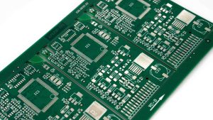
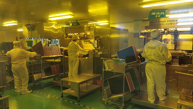
4. PCB Fabrication
The physical production or fabrication involves several tightly coordinated steps:
- Imaging and printing the circuit pattern onto copper-clad laminate
- Chemical etching to remove excess copper
- Sequential lamination for multilayer PCBs (burying vias, building up the stack)
- Drilling (mechanical or laser for tight microvias)
- Plating through holes and via structures
Processes like laser-drilling and sequential lamination are used for advanced boards and can take longer than simple double-layer boards.
5. Surface Treatment and Solder Mask Application
The selection of surface finish determines the long term reliability of the equipment as well as manufacturing efficiency. Common processes include hot air solder leveling (HASL), electroless nickel immersion gold (ENIG), and immersion silver (ImmAg), each requiring specific process time. Custom gold plating or special surface finishes involve additional manufacturing steps.
The solder mask completes its application process first, with the silkscreen layer subsequently printed on top of the solder mask’s surface. The solder mask covers the circuit board substrate and exposes the component soldering locations precisely, while the silkscreen layer prints component identification symbols and product marking text onto the board surface.
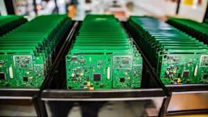
6. PCB Assembly
After the bare board is fabricated, the process moves to component placement and soldering. The assembly process undergoes automated pick-and-place machine operations for component positioning, followed by reflow or wave soldering for component fixation. Assembly time is determined by component supply lead times, total production batch quantities and circuit board design complexity, while also being influenced by whether testing procedures and AI visual inspection processes are included.
7. Inspection, Testing and QA
Automated optical inspection equipment scans the circuit board, X-ray inspection machines examine BGA solder joints, and in-circuit testers along with flying-probe testers verify electrical connection performance and detect existing defects. PCB products applied in demanding fields such as automotive and medical sectors must undergo more rigorous testing procedures, including thermal cycling tests and impedance testing items.
8. Packaging & Shipping
Packaging for anti-static security, just-in-time (JIT) inventory models, and global PCB shipping options all play roles in the final project duration.
Prototype PCB Manufacturing: Speed vs. Accuracy
Manufacturers emphasize their rapid prototyping capability. The factors that actually determine whether the prototype delivery timeline is 24 hours or one week include the following key items.
- Project Scope:A simple single-layer circuit can sometimes be fabricated within 24 hours, especially when using standardized options.
- Design Complexity:Irregular board edges or buried vias require more setup.
- Component Availability:All electronic components must be sourced. Special microcontrollers or legacy parts may delay assembly.
- Quality vs. Speed:Faster turnaround times may come at the expense of certain surface finishes or in-depth testing.
Full-Scale PCB Production and Assembly: End-to-End Timelines
During the transition from prototype to mass production, fundamental changes occur in production objectives and requirements. The core focus of mass production is repeatable manufacturability, production cost control and supply chain flexibility. The final solution must be equipped with production capacity to meet global market demand.
| Production Phase | Typical Duration | Factors that Influence |
| Final Design Validation | 1–3 days | Documentation completeness, compliance |
| Material Procurement | 2–10 days | Substrate type, copper/thickness, quantity |
| Fabrication (Bare Board) | 3–15 days | Layers, buried/blind vias, microvias, size |
| PCB Assembly | 1–5 days | Component sourcing, part count, SMT/THT |
| Testing/Inspection | 1–3 days | QA level, AOI, functional/thermal tests |
| Packaging & Shipping | 1–3 days | Device destination, logistics choice |
Factors That Influence PCB Manufacturing and Assembly Times
Many things can speed up or delay PCB manufacturing:
- Board Complexity:
- Multi-layer, dense via fields or embedded passives slow fabrication.
- Simple, single-layer PCBs can be produced much faster.
- Production Volume / Batch Size:
- Prototyping small runs is quicker but less cost-effective per unit.
- Large batches benefit from scale, but increased production time.
- Supply Chain and Component Sourcing:
- Popular, in-stock parts result in faster assembly.
- Hard-to-find, legacy or specialty components can bring production to a halt.
- Manufacturing Capability:
- Not all manufacturers are equally capable—some struggle with tight tolerances or advanced HDI builds.
- Choose manufacturers with a track record fabricating boards like yours.
- Testing & Compliance:
- QA steps like functional test or environmental stress-screening ensure reliability but add time.
- Documentation and Design Quality:
- Incomplete files or errors during the design file delivery phase lead to an interruption in the manufacturing process. Manufacturers pause operations to await clarification of the issues, a process that extends the delivery timeline.
Typical Turnaround Times for Different PCB Applications
Turnaround time for PCB manufacturing exhibits significant variation. This variation in turnaround time is determined jointly by the circuit board’s application, design parameters, fabrication technology and assembly requirements. Common scenarios include the following.
1. Simple Consumer Device Prototypes
- Basic bare board (e.g., wearables, fitness trackers): 24 hours–3 days
- Assembly with in-stock components: Add 1–2 days
2. Smartphone & Mobile Device Circuit Boards
- Multi-layer HDI printed circuit boards (PCBs) are the backbone of modern smartphones.
- Fabrication: 5–8 days for prototype; 7–20 days for full-scale production with advanced features like buried or blind vias.
- Assembly and testing: 2–5 days (often prioritized for faster market entry)
3. Industrial or IoT Applications
- Boards that demand tighter tolerances, thermal management (aluminum/copper substrate), and reliability can take longer.
- Fabricate and assemble: 7–15 days (especially with high mechanical or environmental requirements)
4. Automotive/Medical/Rugged Applications
- Application often dictates extra compliance and inspection procedures.
- From submission to delivery: 10–25 days for full qualification, sometimes longer for global logistics or advanced functional testing.
Average PCB Manufacturing & Assembly Durations by Application
| Application | Prototype (Bare Board) | Full Production | Assembly/QA |
| Consumer Electronics | 24–72 hours | 3–7 days | 1–2 days |
| Smartphones | 3–5 days | 7–20 days | 2–5 days |
| Industrial/IoT | 3–7 days | 7–15 days | 2–4 days |
| Medical/Automotive | 5–10 days | 10–25 days | 3–7 days |
Tips for Faster PCB Manufacturing and Quicker Prototyping Stages

Rapid prototyping and quicker production time can make all the difference, especially when innovation cycles are tighter than ever. Here’s how to optimize:
1. Align Design With Manufacturer Capabilities
- Stick to preferred stack-ups, drill sizes, and trace widths for the facility you choose.
- Consult DFM checklists to avoid costly feature changes during manufacturing.
2. Standardize Electronic Components Wherever Possible
- Choosing components that are common and always in stock shortens assembly time.
- Define alternates in the BOM so manufacturers can substitute immediately if a part runs out.
3. Use Rapid PCB Services for Prototypes & Iterations
- Many capable facilities offer expedited options—getting bare boards or even full assemblies in as little as 24 hours.
- For first-article boards, prioritize speed over small cost savings; the learning you gain is invaluable.
4. Optimize Your Documentation
- Double-check Gerber files, drill files and BOM for errors.
- Clearly note parameters for surface finish, solder mask, layer stack-up and test requirements.
5. Plan for Parallel Processes
- Begin electronic component sourcing at the same time as bare board fabrication.
- Use modular test fixtures to allow electrical testing immediately after assembly.
Common Mistakes That Can Take Longer to Fix
Avoiding these errors is essential to reliable, quick PCB turnaround times:
- Submitting Incomplete Files:Missing parameters, ambiguities in the BOM or layout errors force manufacturers to pause—every clarification takes extra hours or days.
- Selecting Uncommon or Obsolete Parts:These can delay assembly as procurement searches for alternatives or waits for long lead-times.
- Ignoring DFM Feedback:If a design isn’t manufacturable as received, expect delays for revision and re-fabrication.
- Lack of Consideration for Application:Not all circuit boards for device applications are equal—harsh environments, high current or tight tolerances demand extra QA.
Best Practices and Key Considerations for PCB Projects
To maximize success and minimize risk in PCB manufacturing, consider these best practices:
- Early Vendor Engagement:Work closely with suppliers who are capable of both quick-turn and full-scale production—it enables seamless transition from prototype to launch.
- Design for Scalability:If your final product will scale, avoid custom features in early versions unless essential.
- Track Every Parameter:From copper thickness to mask color, clear communication of every consideration avoids errors and rework.
- Batch Similar Projects:If you develop multiple device variants, batch them to benefit from faster, more cost-effective manufacturing.
- Account for Testing:Applications with higher risk (healthcare, automotive) require additional validation—don’t shortcut QA to save hours if the risk is unacceptable.
- Continuous Learning:After every project, document lessons learned to streamline future designs and processes.
Conclusion & Future Trends in PCB Services
PCB manufacturing processes support technological innovation activities, support rapid prototyping verification processes, and support high-volume device production tasks. Starting from layout design, proceeding through bare board fabrication and component assembly, and culminating in final testing and shipping, the duration of each phase is determined by multiple factors. These factors include supply chain response speed and supply assurance capability, supplier process level and technical expertise, as well as design parameter adjustment and iteration efficiency.
Future trends include:
- Smarter Manufacturing:AI-driven inspection, IoT-enhanced process monitoring, and flexible, distributed fabrication facilities for even quicker solutions that meet changing market needs.
- Greater Standardization:To handle global demand, many manufacturers are automating their systems for standard builds, allowing for quicker, more predictable turnaround times.
- Sustainability:Eco-friendly materials and processes are increasingly prioritized, as environmental considerations become as important as speed and cost in PCB projects.