Introduction: V-Cut, PCBs, and Panelization for Modern Electronics
In the fast-paced world of the pcb industry, manufacturing efficiency, product quality, and reliability are more important than ever. Whether designing a simple printed circuit board or assembling HDI (high-density interconnect) circuits packed with surface mount electronic components, how you separate individual boards—known as depaneling—directly impacts yield, cost, and downstream product development.
V-cut technology and v-scoring have become the go-to pcb separation method for achieving precision separation of pcbs from large, panelized arrays. This comprehensive guide explores the manufacturing process, techniques like mouse bites, and best practices that enable superior board edge quality, minimal burrs, and robust yields for both large-scale and prototype production.
PCB Manufacturing Process: V-Cut’s Role in the Printed Circuit Industry
The journey of a printed circuit board from design to final assembly is complex, involving substrate preparation, copper patterning, drilling, plating, assembly, and finishing. One of the final—yet most crucial—steps in this chain is pcb separation, where the panel of boards, known as a PCB panel, is split into its individual units.
Why Panelization and V-Cut are Critical
Panelization is the grouping of multiple small or medium-sized PCBs into a single, larger fabricated panel. This technique:
- Facilitates high-efficiency SMT (surface mount technology) processing and automated handling;
- Streamlines automated optical inspection (AOI), reflow soldering, and final test;
- Reduces wastage and lowers production costs by maximizing raw material use.
The v-cut process—where a precise, shallow V-shaped groove is milled or scored across the circuit board—serves as both a mechanical “break line” and a board separation method. This enables the panelized board to be easily separated without excessive force, stress, or need for advanced tooling.
Understanding the V-Cut Process: PCB Depaneling with Precision

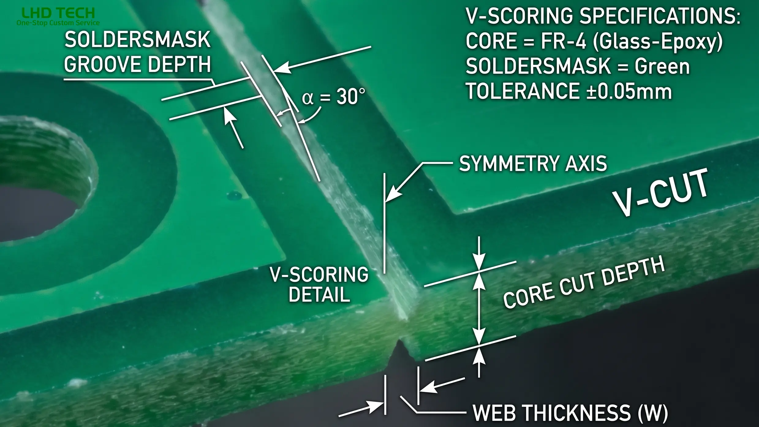
The v cut pcb process involves careful engineering and manufacturing, balancing groove depth, v-cut angle, and residual substrate integrity.
The Steps in the V-Cut Process
Design and Gerber Preparation:
- Engineers specify V-groove locations, typically on a dedicated mechanical or drill drawing layer.
- Panel outline, v-cut lines, and tooling holes/fiducials are added to the PCB manufacturing files.
- It is crucial to maintain recommended clearances: at least 0.5mm (for prototypes) to 1mm (for production) between v-cut lines and any copper or surface mount components.
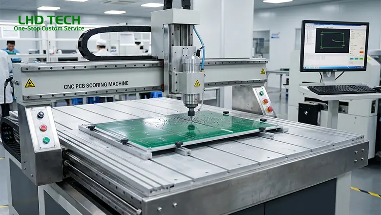
Scoring on Fabrication Line:
- A milling tool or scoring machine with a V-shaped cutting blade incises the board to a controlled, shallow depth (usually leaving 0.5–1.0mm for typical FR-4).
- Both single- and double-sided v-scoring may be used depending on board thickness (double-sided allows for thicker, more robust pcbs).
Post-Scoring Inspection:
- High-quality PCB operations include groove depth and v-cut angle inspection using calibrated gauges.
- Additional check for groove alignment to fiducials/tooling holes to prevent misalignment during depaneling.
Depanelization:
- During or after SMT assembly, the array is separated—either via manual breaking, a dedicated v-cut machine, or fully automated separator.
- Care is taken to avoid mechanical stress on board edges or surface mount components near the v-scored groove.
V-Scoring in PCB Manufacturing: Technique, V-Cut Angle, and Equipment
What is V-Scoring?
V-Scoring is a technique where V-shaped grooves are produced in the substrate to enable easy, controlled snapping of the boards during depanelization. These grooves make it possible to precisely separate boards in large-panelized arrays without excessive damage or burrs.
V-cut angle (30°, 45°, 60°):
- A 45° v-cut angle is most popular for general work, balancing board strength and ease of breaking.
- 30° provides a tighter, stronger joint where needed; 60° is easier to separate but slightly weaker.
Equipment Used
Scoring Machine:
- High-precision scoring machines feature CNC-guided cutting wheels.
- Smaller operations might use manual v-cut machines or even specialized hand tools for prototype runs.
Milling Tool/Blade:
- Carbide or diamond-tipped tools are preferred for advanced materials (e.g., aluminum-backed LED boards).
- For HDI applications, tighter control and optical verification of groove placement is required.
V-Scoring and High-Volume Manufacturing
Automated lines with integrated depanelizers enable millions of pcbs to be efficiently depanelized with minimal operator involvement and near-zero variation in board edge quality.
Benefits of V-Cut for Circuits: High Manufacturing Efficiency & Clean Board Edges

What makes v-cut boards the most popular method of separation for modern high-quality PCB production? Here are the main advantages, relevant for both PCB design and manufacturing:
High Manufacturing Efficiency:
- Fast processing for large panel arrays.
- Minimal operator skill needed; clean board edges achieved even by less experienced staff.
Precision and Clean Board Edges:
- The V-groove creates a nearly burr-free edge; subsequent assembly and fitment require little or no rework.
- Board outline is perfectly linear—a requirement in automated handling.
Low Mechanical Stress:
- V-cutting minimizes the force transmitted to sensitive surface mount pads and electronic components, protecting solder joints and increasing yield.
- Essential in small-pitch HDI and BGA circuits.
Cost-Effectiveness in PCB Manufacturing and Assembly:
- Less tooling wear and waste versus milling instead, making it a more cost-effective board separation method.
- Maximizes raw material use via dense panelization layouts.
Easy for Prototyping and Production:
- Can be designed for quick hand separation in small runs (if board thickness and groove specs are optimized—see “tip” below).
Panelization Layout for PCBs: Best Practices, Tooling Holes, and Board Outlines

Achieving panelization that enables efficient v-cutting and maximum manufacturing efficiency requires careful attention to layout details, use of tooling holes and fiducials, and adherence to recommended separation lines.
Best Practices for Panelization Layout
Uniform Board Outlines:
- Design panel arrays with straight, regularly spaced rows and columns—this ensures grooves are continuous and eliminates unnecessary V-cut starts or stops.
- Avoid designing board edges with arcs or curves where v-scoring is called for. V-cut works best with linear edges; if arcs or complex shapes are needed, use routing or laser cutting instead.
Tooling Holes and Fiducials:
- Locate tooling holes outside of the v-scored regions to prevent weakening panel integrity.
- Place global and local fiducials for vision alignment, particularly if high-speed SMT assembly is planned.
Spacing and Grooves:
- Maintain a minimum spacing of 0.5mm between adjacent board edges, though 1mm is more robust and preferred for high-pressure, thick, or multi-layer boards.
- For multi-row layouts, consider breakaway rails on panel edges for structural support throughout the manufacturing process.
Surface Mount Component Clearances:
- Leave at least 1mm clearance (preferably more for large or tall packages) between the V-groove and any surface mount or through-hole component to prevent mechanical stress during depaneling.
Sample Panelization Layout for 0.8mm and 1.6mm Boards
| Board Thickness | Minimum Groove Residual | Edge Clearance | Surface Mount Clearance | Recommended V-Cut Angle |
| 0.8mm | 0.3–0.4mm | 0.5mm | 1.0mm | 45° |
| 1.6mm | 0.7–1.0mm | 1.0mm | 1.5mm | 45°/60° |
Alternative PCB Separation Methods: Mouse Bites, Routing, and Laser Cutting
While v-scoring is the preferred separation method for many high-volume and prototype PCB projects, there are scenarios where other methods—such as mouse bites or routing—are preferable.
Mouse Bites (Breakaway Tabs)
How Mouse Bites Work:
- Small, drilled holes (“mouse bites”) are placed along a perforated line, connecting the PCB to its panel with thin bits of material.
- During depaneling, these tabs are broken off, often leaving rougher board edges requiring post-separation cleaning.
When to Use Mouse Bites:
- Boards with irregular or curved outlines where v-scoring isn’t possible.
- Small or batch volume projects where specialized v-cut machines are unavailable.
Routing and Milling Instead of V-Cut
- Routing uses a high-speed milling tool to completely separate the board outline, allowing arbitrary shapes but at higher cost and with more edge burrs.
- Best Use Cases:
- Prototypes that require non-linear shapes.
- Surface mount circuits with board edges that include arcs, slots, or internal cavities.
Laser Cutting
- Laser technology offers a precision, no-contact separation technique, ideal for ultra-thin, high-density, or non-standard materials.
- Drawbacks:
- Higher equipment costs.
- Lower throughput compared to v-cut for standard FR-4.
Troubleshooting V-Cut Boards: Common Issues, Edge Quality, and Solutions
Correctly applied v-scoring ensures smooth depaneling. However, poorly controlled groove depth, misaligned v-cut lines, or insufficient clearances can lead to:
Common V-Cut PCB Troubles
Edge Delamination or Burrs:
- Check that the milling tool or scoring blade is sharp and not worn.
- Review v-cut angle and residual thickness—too thin means premature breakage, too thick means excessive force and splintering.
Pad/Trace Cracks Near Board Edge:
- Increase copper clearance from the groove; reroute traces away from V-cut regions.
- For 0.8mm or thin circuits, use double-sided scoring and support the board when breaking.
Component Stress or Detachment:
- Increase component-to-groove distance.
- For high-pressure or thick boards (≥1.6mm), always depanelize using a mechanical fixture or v-cut machine.
Irregular Groove Depth in HDI or High-Layer PCBs:
- Ensure CNC scoring machines are properly calibrated for varying stackups.
- Inspect with a groove depth gauge across the panel to check for variance.
Advanced Depaneling: Scoring Machine, Laser Cutting, and High-Quality PCB Solutions
Advanced manufacturing lines for pcb design and manufacturing are equipped to tackle a wide range of materials, layouts, and application needs:
CNC-Driven Scoring Machines
-
- Support variable groove depths, programmable v-cut angles, dynamic compensation for board bow, and automated fiducial alignment—ideal for large volume, high-density circuits.
Integrated Laser Cutters
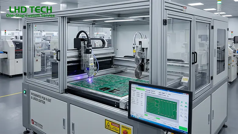
-
- Increasingly used for high-value or micro-PCBs, ensuring no physical contact, ultra-precise edges, and minimal dielectrics chipping.
Guidelines for High-Quality PCB and V-Cut Boards
- Always validate tooling holes and fiducial marks for both v-cut and subsequent assembly lines.
- When designing board outlines involving arcs, combine v-cut for main separation with routing or laser for complex features.
- Specify expected surface finish quality and acceptable edge burr tolerance in your fabrication notes.
FAQs on V-Cut, V-Scoring, and PCB Separation Methods
Q: What is the minimum board thickness recommended for V-cut boards?
A: While double-sided v-scoring is possible down to 0.8mm, best edge quality and mechanical strength are achieved at 1.0mm or above.
Q: Can V-scoring be used on all board materials?
A: It is ideal for FR-4 and standard rigid circuits. For aluminum-backed, ceramic, or flex boards, consult your pcb manufacturer—scoring may require specialized tooling or an alternative method.
Q: How does v-scoring compare to mouse bites in terms of strength and cleanliness?
A: V-cut yields smoother, stronger board edges and is preferred for high-quality, high-yield runs. Mouse bites are reserved for curves, prototype, or areas unsuitable for straight-line v-scoring.
Q: Do I always need post-break sanding?
A: Not with properly tuned v-scoring and a sharp, well-maintained cutting tool. Mouse bite or routed edges generally do require light sanding.
Q: What’s the impact of improper tooling holes or fiducials?
A: Misplaced holes/fiducials can lead to misaligned grooves and defective separation—always double-check placements in your Gerber viewer before fab release.
Conclusion: Innovative Solutions for High-Quality V-Cut PCBs & Product Development
V-cut and v-scoring have become cornerstones of efficient, high-quality printed circuit manufacturing. The right combination of groove depth, panelization layout, v-cut angle, and manufacturing expertise allows designers and engineers to depanelize with confidence—delivering robust, perfectly separated boards for subsequent assembly, surface mount, and final product development.
By understanding all available pcb separation methods—including v-cut, mouse bites, routing, and laser cutting—you’re equipped to select the best solution for any application, whether tight-pitch HDI, odd-shaped boards, or flexible prototypes. As technology and pcb manufacturing and assembly evolve, leveraging the strengths of v-scoring and related innovative solutions will set you apart—giving you an edge in both product development speed and finished board quality.
When you collaborate with a pcb manufacturer with advanced v-cut process capabilities, you unlock the full potential of high-quality PCB production, confident that every panelized circuit board will separate cleanly and predictably—whether it’s a tightly nested HDI array for consumer electronics or robust automotive PCBs demanding tough, consistent board edges.
Final Tips for Maximum Manufacturing Efficiency
Start with the Right Design:
- Always specify exact v-cut groove locations, panel size, and fiducials/tooling holes in your design and manufacturing process documentation.
- Work with your fabricator to optimize the board separation method for your unique product.
Use the Best Tools and Equipment:
- Whether it’s a manual v-cut machine, automated scoring machine, or even laser cutting for exotics, the right tool ensures the precision your boards require.
Maintain DFM (Design for Manufacturability) Best Practices:
- Factor in v-cut angle, groove depth, component clearance, and support rails early on.
- For complex geometries or edge with arcs, don’t force v-scoring—use milling instead for those regions.
Do a Small Pilot Run:
- Before moving to mass production, run a handful of panels to test the separation method.
- Inspect board edges, check for pad or trace lifting, and validate the ease of depaneling during subsequent assembly.
- Adjust your cutting tool or v-cut process as needed.
Keep Learning:
- The pcb industry is continuously seeking even better ways to balance cost, throughput, and quality. Stay current with the latest developments in v-cutting, scoring technology, and hybrid PCB separation methods by networking with suppliers and attending industry conferences.