Introduction
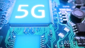
The continuous evolution of electronic devices has driven the ever-growing demand for higher data transmission speeds, superior signal integrity and enhanced system reliability. Devices operating in high-frequency environments include 5G base stations, wireless communication systems, radar systems and high-end medical electronic equipment, all of which impose special requirements on circuit boards—requirements that traditional single-material printed circuit boards are often unable to meet.
Hybrid PCBs have rapidly become the go-to solution for solving intricate performance challenges, especially in environments where signal loss and better impedance control, high thermal conductivity and complex mechanical properties are required. A hybrid circuit board is constructed by combining two or more different materials into a single stack-up, taking advantage of the strengths of each substrate. Today, hybrid printed circuit boards are used to satisfy increasing expectations for long-term reliability and high-frequency performance in a wide range of applications, from consumer electronics to mission-critical systems in aerospace.
In this comprehensive guide, we’ll uncover why the demand for hybrid PCBs is surging, the key advantages of hybrid PCBs in high-frequency circuit design, how these boards are made, the common materials used in hybrid PCB construction, best practices for hybrid PCB design, and what makes hybrid PCB manufacturing an absolute game-changer for electronics.
What Are Hybrid PCBs?

Hybrid PCBs, also referred to as hybrid material PCBs or hybrid circuit boards, are an innovative type of printed circuit board. They are characterized by the incorporation of two or more distinct base materials within the laminate stackup of a single circuit board. This hybrid structure enables each circuit layer to leverage the optimal electrical performance and thermal characteristics of the material it is fabricated from. As such, Hybrid PCBs are well-suited for applications where the required circuit performance exceeds that achievable with conventional FR4 substrates.
Typical hybrid PCB structure:
| Layer | Substrate/Material | Functionality |
| Top Layer | PTFE | High-frequency signal transmission |
| Middle Layer | FR4 | Mechanical support, routing |
| Interior Layer | Ceramic | Heat dissipation, electrical insulation |
| Flex Section | Polyimide | Flexibility for moving/bending regions |
| Bottom Layer | FR4 | Structural stability |
Hybrid PCBs adopt a solution that integrates multiple materials, which possess distinct electrical and mechanical properties. This thus enables designers to perform precise optimization for specific performance metrics, such as enhancing signal integrity, improving thermal management efficiency, boosting mechanical structural strength and enabling more flexible routing design.
Why Use Hybrid PCBs?
Hybrid PCBs are widely used in situations where individual materials would not provide sufficient performance. For example, PTFE offers ultra-low dielectric loss for high-frequency layers, while FR4 brings good mechanical strength and cost-efficiency, and polyimide delivers flexibility in dynamic or foldable regions. By combining them with the superior properties of ceramics or metal cores for heat management, you can create hybrid pcbs that excel in a wide range of applications.
Why Hybrid PCBs Are Critical for High-Frequency Applications
The High-Frequency Challenge
In the current field of electronic technology, high-frequency circuits typically refer to circuit systems with operating frequencies exceeding 500 MHz. Their frequency range can extend to the GHz level. Such circuits are widely used in scenarios such as digital communication, radar systems and advanced radio frequency electronic equipment. An increase in operating frequency leads to greater signal loss. It also raises the risk of crosstalk between signals. Electromagnetic interference issues become correspondingly more pronounced. These factors collectively threaten signal integrity. Ultimately, they can also impact the overall performance of the device.
Printed circuit boards used for high-frequency digital circuits must provide:
- Low dielectric loss and consistent Dk/Df for fast, clean signal transmission
- High thermal conductivity to remove heat from high-power components
- Good mechanical properties to withstand vibration, shock or dynamic flexing in harsh environments
- Electrical insulation and controlled impedance to prevent signal reflection, unwanted coupling and data integrity loss
How Hybrid PCBs Help
Hybrid PCBs effectively mitigate these risks through targeted material combinations. High-frequency signal traces can be routed on polytetrafluoroethylene substrates, a material that significantly reduces signal loss and enables more precise impedance control. The main structural support of the circuit utilizes FR4 substrates, which offer better cost-effectiveness. Ceramic thermal conductive layers provide excellent heat dissipation capabilities. Polyimide flexible materials are suitable for areas of the device that require bending or folding, with typical applications including wearable devices and compact integrated assemblies.
Hybrid PCBs possess both flexibility and high performance. These two attributes are crucial for meeting contemporary industry standards. This material finds extensive application across various high-end products such as wireless base stations, ADAS radar modules, medical implant devices with integrated RF functionality and IoT sensors.
Advantages of Hybrid PCBs in High-Frequency Circuit Design

1. Increased Signal Integrity and Transmission Quality
Hybrid circuit boards employ specific design methods by arranging high-frequency signal layers on polytetrafluoroethylene or similar high-performance materials. This design effectively reduces energy loss, signal reflection, and impedance mismatch during signal transmission. Such technical treatment plays a crucial role in ensuring the data accuracy and transmission rates of gigahertz-level circuits.
2. Superior Thermal Management
The materials used in hybrid PCB production possess distinct characteristics. Beneath high-power-density components, ceramic or metal materials are typically employed as the core layer. This structure exhibits the physical property of high thermal conductivity and enables rapid heat dissipation. This characteristic effectively protects sensitive integrated circuits within the circuit. It also contributes to extending the practical service life of electronic components. Furthermore, the operational performance and reliability of the overall system are enhanced as a result.
3. Mechanical Strength and Rigid-Flex Versatility
Hybrid PCBs achieve specific functions through a rigid-flex design approach. The rigid PCB sections primarily deliver required mechanical support strength and circuit electrical stability. The flexible areas utilize polyimide material to enable bending or folding capabilities. This integrated structure creates feasible hybrid design solutions for device assembly within three-dimensional space and components with motion requirements. Such designs can withstand harsh operating conditions such as vibration and impact. They also meet the stringent demands of modern consumer electronics for internal space compactness.
4. Cost-Effectiveness and Functional Integration
Hybrid circuit board manufacturing adopts a selective material allocation scheme. This method utilizes high-performance materials in critical areas and employs cost-effective substrates in other regions. Such an approach effectively controls the cost of multilayer PCB applications and prevents excessive increases in project budgets. Hybrid PCB technology enables the integration of analog circuits, digital circuits, RF modules and power management functions onto a single circuit board. This integrated design significantly reduces the complexity of internal interconnections within the system while also lowering the overall structural weight.
5. Long-Term Reliability
Designing hybrid PCBs requires matching the thermal expansion coefficients of materials, optimizing their electrical properties, and ensuring their environmental resistance. Proper selection of these key material properties ensures the long-term stable operation of devices, even when they are deployed in the harsh operating environments typical of the automotive, aerospace and medical device industries.
Common Materials Used in Hybrid PCB Manufacturing
The materials selected for hybrid PCB assemblies directly determine their electrical performance and thermal management performance. In the current industry, the most common material selections are as follows:
| Material | Key Property | Typical Use in Hybrid Circuit Board |
| FR4 | Good mechanical, cost | Support, routing, structural layers |
| PTFE | Low dielectric loss | High-frequency signal layers |
| Ceramic | High thermal conductivity, insulation | Heat spreaders, power modules |
| Polyimide | Flexible, heat-resistant | Dynamic or moving circuits (rigid-flex) |
| Metal core (Al, Cu) | Conductive, dissipates heat | Power conversion, LED backplanes |
Why PTFE and Ceramic Stand Out
- PTFE offers unrivaled signal integrity for microwaves and millimeter-wave digital circuits. Used in hybrid PCBs for base stations, satellite communication and cutting-edge consumer electronics.
- Ceramic—with its superior electrical insulation and high thermal conductivity—is essential for reliable operation in high-power and extreme temperature environments, such as automotive radar systems or aerospace navigation modules.
- Polyimide: Chosen for bending and dynamic applications, making it perfect in the production of hybrid PCBs for wearables.
Key Hybrid PCB Design Considerations
Stack-Up and Impedance Control
- Hybrid PCBs combine multiple materials:Every transition between materials in a stack-up affects impedance. Use simulations and close cooperation with your hybrid PCB manufacturer to ensure controlled impedance along all high-frequency routes.
- Keep high-speed signals on low-loss layers, and utilize ground planes and shielding techniques.
Coefficient of Thermal Expansion, Mechanical Properties
- Mechanical properties, especially CTE,are paramount. Choose materials for hybrid PCBs that expand at similar rates to avoid warping.
- Multilayer circuit board designs must maintain mechanical symmetry. This symmetrical design prevents internal stresses caused by temperature variations during both the manufacturing phase and operational periods. The requirement for mechanical symmetry holds particular importance for hybrid PCB designs. Such designs involve combining two substrates with entirely different properties, such as PTFE and FR4.
Hybrid Circuit Board Routing and Layer Allocation
- For signal transmission, route high-frequency signals on PTFE or similar low dielectric loss substrates.
- Use FR4 or other sturdy substrates for power and ground distribution, as well as regions demanding structural support.
- Separate analog, digital, and RF routing to minimize cross-interference—a benefit only possible through the versatility of hybrid pcbs.
Sourcing and PCB Assembly
In hybrid PCB manufacturing, components and materials should be procured at an early stage. This is due to the potentially extended lead times of specific substrate types such as ceramic substrates or high-frequency PTFE. Modern assembly and reflow processes impose strict requirements: all component heights must remain uniform, and the Z‑axis coefficient of thermal expansion must be matched consistently.
Applications: Where Hybrid PCBs Are Widely Used
Hybrid PCB technology addresses both design challenges related to electrical performance and mechanical structure. This capability enables its wide application in various fields, including compact devices, rugged products and high-performance electronic systems.
| Application Area | Examples of End Products | Why Use Hybrid PCB Here? |
| Telecommunications/5G | Base stations, repeaters, antennas, fiber comms | Minimizing signal loss; robust, outdoor reliability |
| Consumer electronics | Gaming consoles, smart TVs, high-speed routers | Miniaturization, high-speed digital circuits |
| Automotive/ADAS | Radar/lidar, cameras, ECUs, infotainment, power modules | Vibration/shock resistance, heat management |
| Aerospace/Defense | Avionics, radar, guidance, navigation, satellites | High-frequency performance; reliability tests |
| Medical devices | Imaging, monitoring, implants, wearables | Bio-compatible flex, compact, EMI shielding |
| IoT/Wearables | Fitness trackers, remote sensors, smart fabrics | Flexible sections, wireless communication |
| Power electronics | LED drivers, converters, chargers | Ceramic/metal-core for thermal paths |
In digital circuit design for high-speed routers, hybrid PCBs are extensively utilized. This design effectively controls signal attenuation while significantly enhancing electromagnetic interference suppression capabilities. High-end automotive electronics applications similarly rely on hybrid PCB technology, with typical use cases including hybrid electric control units and battery management systems. This technology enables circuit boards to maintain stability in harsh operating environments while achieving the dual objectives of miniaturization and high reliability. Medical electronic devices are evolving toward greater compactness, integration and wearability, which directly drives a rapid increase in market demand for hybrid PCBs.
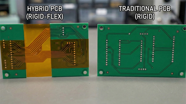
Hybrid PCBs vs. Traditional Circuit Boards
When evaluating whether to use hybrid PCBs for your next project, consider the following:
| Feature | Standard PCB | Rigid-Flex PCB | Hybrid PCB |
| Substrate | Single material | Flexible + rigid | Multiple materials (e.g., PTFE+FR4) |
| Performance | Limited by one material | Good for motion | Tuned for electrical/mechanical needs |
| High-frequency use | Poor | Good (if proper material selected) | Exceptional (uses optimal stack-up) |
| Cost efficiency | Great for simple, low-cost | Higher | Best for complex, multi-function boards |
| Application scope | Low-medium complexity | Dynamic applications | Wide range: telecom, IoT, automotive, aerospace |
| Reliability | Good | Good | Best (long-term, harsh conditions) |
Hybrid circuit boards integrate the dual characteristics of rigid-flex structures and advanced materials. This integration grants engineers greater design freedom over circuit performance and cost control. Such circuit boards demand more precise manufacturing processes and assembly techniques. They demonstrate notable advantages in three key dimensions: high-frequency signal transmission, long-term operational stability and component miniaturization. This comprehensive superiority is difficult to achieve with traditional circuit boards.
Hybrid PCB Manufacturing Process & Tips
The manufacturing process for hybrid PCBs is more complex than that for standard PCBs, a complexity that stems from the combination of multiple materials used. Producing these boards therefore requires more meticulous planning and strict control over processes.
- Design Phase:Layout stack-up with the help of your manufacturer. Specify the exact laminates, copper weights, and prepreg materials used in hybrid PCB sections.
- Material Procurement:Order all different materials early—lead times for high-frequency laminates or ceramics may be several weeks.
- Lamination:Special processes may be needed for combining different materials. Controlled heat/pressure cycles minimize warping and ensure adhesion.
- Drilling & Routing:Advanced multi-head drills and laser cutters are often used for complex hybrid or rigid-flex PCBs, which require precise via alignment.
- Assembly:Match solder profiles and AOI/ICT test fixtures to the mechanical and thermal behaviors of each hybrid section.
- Testing:Use microsection analysis, TDR (Time Domain Reflectometry), thermal cycling and functional end-of-line testing to ensure performance and reliability.
Industry Trends & Future of Hybrid PCBs
The Expanding Use of Hybrid PCBs
- Hybrid pcb design is driving growth in consumer electronics and automotive electronics as AI, wireless communication, and sensor integration deepen.
- Next-gen hybrid pcbs may include embedded capacitors, inductors or even microfluidic channels in medical and IoT devices.
- As digital circuits operate at ever higher frequencies, low dielectric loss and fine-tuned impedance are now essential in even mid-tier products.
Future Innovations
- Research is ongoing into new materials for hybrid structures, such as nano-ceramics, improved flexible copper-clad laminates, and eco-friendly polymers.
- Printed circuit board fabrication will continue to automate, with real-time digital QA, AI-driven process optimization, and direct-write 3D PCB prototyping for hybrid designs.
Frequently Asked Questions
What are the main advantages of hybrid PCBs for high-frequency circuits?
Hybrid pcbs combine multiple materials, such as PTFE, FR4, and ceramic, to yield low signal loss, optimized impedance, high thermal conductivity and mechanical strength. Hybrid pcbs offer tailored solutions for demanding RF and digital circuits.
What are the common materials used in hybrid PCBs?
Common materials used in hybrid pcb designs include FR4 (mechanical/lower cost), PTFE (high-frequency/low loss), ceramic (thermal paths), polyimide (flexibility) and metal cores (heat dissipation). The choice depends on performance requirements.
Are hybrid PCBs good for multilayer pcb applications?
Yes, hybrid pcbs are widely used for complex multilayer applications, such as those found in wireless communication, automotive radar and IoT sensor devices. Their ability to combine different materials gives them a unique advantage in space-saving, reliability and high-frequency performance.
Why use hybrid PCB instead of standard rigid or rigid-flex?
Hybrid circuit boards enable each region of the board to have the best possible electrical and mechanical properties for its purpose — without overengineering with costly material everywhere. This approach improves cost-effectiveness and enables designs not possible with single-material PCBs.
What industries demand hybrid pcbs most?
Telecommunications, automotive (especially for ADAS/ECU), aerospace and defense, medical electronics, consumer electronics and IoT/wearable devices are all sectors driving increased hybrid PCB production.
Conclusion
The production of hybrid pcbs represents a major step forward in the evolution of electronics. By allowing designers to combine multiple materials in one printed circuit, hybrid pcbs help solve the toughest challenges of high-frequency performance, signal integrity, mechanical strength and electrical reliability, and thermal management. Today, hybrid pcbs are widely used in everything from wearable devices to next-gen radar, making them ideal for a wide range of applications where conventional boards would fail.
With advances in hybrid pcb design, better materials, and continuous improvement in hybrid pcb manufacturing processes, the future is bright for engineers and innovators looking to push the boundaries of what’s possible in electronics.
If you’re developing a new high-frequency circuit, exploring rigid-flex boards, or simply trying to boost the reliability of your pcb design, consider the advantages of hybrid pcbs. Engage early with manufacturing partners, leverage state-of-the-art materials for hybrid construction, and join the next generation of designers who create hybrid pcbs for high-performance, reliability and long-term success.