Introduction: Overview of Multilayer Rigid-Flex PCB Technology
The manufacturing process of multilayer rigid-flex PCBs is propelling a transformation in the production methods of electronic products. This process integrates the high-performance characteristics of multilayer circuits with the high-stability features of the rigid-flex combined structure. Its unique design enables engineers to achieve two key objectives simultaneously: maintaining the high-density wiring layout advantages of rigid circuit boards while possessing the bendable and adaptable physical properties of flexible circuits.
What is a Multilayer Rigid-Flex PCB?

Multilayer rigid-flex PCBs represent a composite electronic circuit architecture. This structure securely integrates rigid substrates and flexible substrates through a lamination process. Copper circuit layers are interposed between flexible polyimide material and FR4 rigid boards, forming an interlaced arrangement. Such a design enables the high integration of complex circuits, thereby meeting the stringent requirements of modern electronic products for compact spatial layouts.
Classic use cases: Aerospace boards, medical imaging devices, foldable phones, automotive control units and IoT sensors—all rely on the process of multilayer rigid-flex board’s unique strengths.
Composition & Structure: Multilayer Rigid-Flex PCB Fundamentals
Core Materials
- Rigid Layers:Typically FR4 or high-Tg epoxy, providing structure for mounting and connectors.
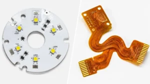
- Flexible Layers:Polyimide (PI) or PET films paired with copper, enabling dynamic flex and routing through tight spaces.
- Adhesive & Bonding Films:Specialized adhesive and pre-preg layers ensure the flex and rigid layers are laminated into a single, high-quality circuit board.
- Coverlays:Polyimide films insulate and protect flexible patterns.
Board Stack-Up
| Layer | Material | Purpose |
| Top | FR4 Copper | Rigid component mounting |
| Inner | Polyimide + Cu | Flexible interconnect, dynamic flex |
| Core | FR4 Copper | Stability, multilayer routing |
| Bottom | Polyimide + Cu | Additional flexible circuit |
Advanced Structural Details
- Multilayer construction:Axis-oriented stacking of alternating rigid and flexible layers.
- Pattern alignment:Critical for complex nets, microvias and fine-pitch SMT pads.
- Hole plating:Mechanical or laser-drilled vias connect each layer, with careful bake and desmear steps before copper plating.
Benefits: Why Choose Multilayer Rigid-Flex PCBs?

- Space and Weight Savings:Miniaturization is crucial in today’s electronics. Rigid-flex circuits eliminate bulky connectors and wires, enabling more functionality in less space.
- Complex Multilayer Design:The ability to route circuitry through both rigid and flexible regions supports high-density, multilayer architectures.
- Enhanced Durability:Flexible layers absorb shocks and vibration, protecting the circuit from physical stress.
- Fewer Failure Points:Integrated layers mean fewer solder joints and connectors, resulting in improved board reliability.
- Superior Mechanical Integration:Boards can handle repeated bending without fracture, perfect for hinged displays or movable medical devices.
Step-by-Step Manufacturing Process of Multilayer Rigid-Flex PCBs

1. Design & DFM Review
- Design:Engineering teams create stack-up diagrams, layer sequences and pattern layouts using advanced EDA tools. Every transition from rigid to flex and every via or connector hole, is mapped.
- DFM Optimization:The design undergoes a thorough DFM review for manufacturability and testability, verifying that the board’s requirements match production realities.
2. Material Preparation & Imaging
- Imaging:Each copper layer is patterned (by photolithography or laser direct imaging) per the design file, establishing intricate circuit patterns on both rigid and flex sections.
- Bake:Core materials and flexible substrates are pre-baked to remove moisture, preventing delamination during lamination.
3. Etching & Inner Layer Fabrication
- The etching process performs the operation of removing excess copper layers, precisely preserving the designed circuit traces. The multi-step etching procedure and imaging technology work in collaborative action to form high-quality, fine-line patterns on multilayer circuit boards.
4. Lamination & Bonding
- Lamination:Rigid and flexible layers are stacked and bonded together with adhesives using high temperature and pressure (often in a vacuum lamination press), resulting in a multilayer board with both rigid and flex regions.
- Alignment at this stage is essential for layer-to-layer registration.
5. Drilling, Plating and Hole Prep
- Drilling:CNC or laser equipment make precision holes for through-connections (vias), connectors and mounting.
- Desmear & Bake:Plasma or chemical processes clean hole walls for optimal plating bond.
- Electroplating:Adds copper to the drilled holes, connecting all the multilayer circuits.
6. Outer Layer Patterning, Solder Mask & Surface Finish
- Outer Imaging & Etching:Defines the final signal/power traces and pads.
- Solder Mask Application:Protects areas not meant for solder and provides electrical insulation.
- Surface Finishing:ENIG, OSP or HASL provide robust solderable surfaces, protecting copper from oxidation.
7. Coverlay, Silkscreen, Profiling & Final Assembly
- Coverlay films are laminated to flexible areas, exposing only pads needed for soldering. Component markings and labeling are applied via silkscreen. Profiling (routing/laser) cuts the entire board to final shape.
- Assembly:High-precision surface mount technology lines carry out the placement and soldering of components, while the flexible sections require specialized support during reflow soldering to manage deformation.
Quality Control, Testing & Certification
Key Steps in Ensuring Board Reliability
- AOI & X-ray Inspection:Scans for misalignment, pattern defects, incomplete vias and soldering faults.
- Electrical Testing:Comprehensive open/short testing of every net—verifying circuit continuity.
- Flex/Bend Testing:Repeated flex cycles simulate real-world handling of flexible layers.
- Environmental & Bake Testing:Boards are baken under controlled humidity and temperature to verify adhesion, bond strength and resistance to delamination.
Common Challenges and Solutions in Multilayer Rigid-Flex PCB Fabrication
Frequent Issues
- Delamination:Solved by proper bake and adhesive selection.
- Pattern Shift:Minimized by tight process controls during imaging and alignment.
- Microcracking in Copper:Prevented through correct copper thickness selection and specifying conservative bend radii in flex areas.
- Hole Wall Defects:Addressed by optimized desmear, cleaning and plating.
Latest Innovations & Industrial Trends
- Fine-Line Imaging & Laser Drilling: Supports higher I/O density in microelectronics.
- Adhesive-Free Flex Cores: Reduce thickness and enhance thermal/mechanical performance.
- Digital Twinning: Virtual simulations of the entire PCB design and process of multilayer rigid-flex fabrication process improve first-pass yield and cut down prototype iterations.
- AI-driven Optical Testing: Automated imaging and inspection systems catch pattern shifts, voids or via defects earlier in production than traditional visual checks.
- Sustainable Materials: The latest research is driving new low-halogen adhesives, recyclable PET-based flexible layers and energy-efficient lamination ovens, supporting both compliance and eco-friendly board production.
FAQs about the Multilayer Rigid-Flex PCB Process
Q: Why use multilayer rigid-flex PCBs instead of just rigid PCBs?
A: Multilayer rigid-flex PCBs not only possess the stable structure and high-density layout capability of rigid circuit boards, but also inherit the space-saving, weight-reducing characteristics of flexible circuit boards while adapting to dynamic bending environments. This hybrid design simplifies complex three-dimensional wiring challenges, reduces reliance on connectors and discrete cables, and thereby enhances the overall reliability of the system.
Q: What PCB fabrication and assembly steps require the most care?
A: Imaging, lamination and hole drilling/plating steps are critical. Flaws during these affect all downstream steps. Carefully controlled bake, adhesive application, alignment and copper plating ensure a robust multilayer bond. Automated testing and AOI verify these aspects throughout production.
Q: How do you handle flex-layer stress during production?
A: Engineering teams specify optimal copper and adhesive thickness, as well as conservative bend radii and route traces along the neutral axis of flexible layers. Boards often undergo flex and bake tests pre-shipment to predict real-world stress impact.
Q: What certifications should my PCB manufacturer carry?
A: Look for ISO, IPC, and, when needed, IATF for automotive. Certification is the difference between a basic board shop and a high-quality multilayer rigid-flex PCB manufacturer.
Selecting a High-Quality PCB Manufacturer & Assembly Partner
The fabrication and assembly processes of multilayer rigid-flex PCBs require that the collaborating party possess specialized process technology, be equipped with top-tier production equipment and enforce strict process control throughout the entire procedure.
What to Look For
- Proven Expertise:Seek out partners with a portfolio of complex multilayer rigid-flex board projects—ask for an overview of multilayer builds previously completed.
- Modern Imaging & Lamination Equipment:Newer vacuum lamination presses and precision imaging equipment ensure superior bond and fine-circuit patterning.
- Flexible Production Lines:Companies experienced in handling both rigid and flexible layers during assembly can better maintain board planarity and correct alignment.
- High-Quality Certification:Always request evidence of board certification and compliance with relevant standards.
- Comprehensive Testing:Ensure your manufacturer includes imaging tests, etch depth checks, bake cycles, hole plating and final electrical verification as standard quality steps.
Choosing a Turnkey Supplier
PCB manufacturers with full-service capabilities provide customers with end-to-end production and technical support, which covers all implementation stages including circuit board design, DFM review, prototype fabrication, volume production, PCB manufacturing and assembly, and post-production testing. The one-stop procurement mode can effectively shorten the overall implementation cycle of projects, it can substantially reduce the overall operational costs of projects, it can create adaptable implementation conditions for the rapid design iteration of products, and the practical application value of the one-stop procurement mode bears crucial practical significance in the electronic market where technologies and market demands are continuously updated and upgraded.
Conclusion: The Future of Multilayer Rigid-Flex Electronics
The technical research overview of multilayer rigid-flex PCBs defines the core technical positioning of the fabrication process for multilayer rigid-flex PCBs, and this process serves as the core technical foundation for the development of next-generation circuit design work. Multilayer rigid-flex PCBs with high-precision engineering achieve an optimal balance effect across multiple key performance dimensions, and these key performance dimensions encompass board flexibility, circuit integration density, board structural strength and the core requirements of product miniaturization design.
Every manufacturing process of multilayer rigid-flex PCBs from design to mass production, covering the entire workflow from imaging, etching, baking, alignment and lamination to final product inspection, requires the implementation of rigorous process control and quality management. Full-process process control and quality management can drive technological innovation and facilitate the miniaturization of products, while enabling electronic manufacturing enterprises to produce compact and high-quality devices—the R&D and production of such devices cannot be realized by virtue of conventional board technology.
Enterprises establish in-depth cooperative partnerships with certified high-quality PCB manufacturers, and these partnerships ensure that the complex circuits of circuit boards have practical capabilities to withstand various application conditions that cover the sustained effects of operational stress, the repeated impacts of dynamic flexing and the multiple challenges of harsh operating environments. The market’s core demands for electronic devices show a steady upward development trend, and such electronic devices need to have more intelligent operational performance, more compact structural form and more reliable service quality. Enterprises firmly master the fabrication processes and assembly processes of multilayer rigid-flex PCBs, and the proficient mastery of such core processes enables enterprises to establish first-mover competitive advantages in the overall development process of the industry.