Introduction to PCBA & Printed Circuit Board Assembly

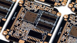
Printed circuit boards serve as both the physical foundation and functional implementation platform for modern electronic devices. A bare board in its unpopulated state possesses no practical functionality. Within a systematic assembly process, various electronic components such as resistors, capacitors and integrated circuits are precisely secured and connected to the board, transforming the static substrate into an operational electronic circuit. Complete PCBA manufacturing begins with design verification and extends to the precise placement and reliable soldering of components. Subsequent testing and validation phases ensure the finished circuit board assembly achieves stable performance and reliable structural integrity, enabling its direct integration into final products for operational use.
PCBA, as a core production technology in electronic manufacturing, is widely applied across multiple critical industries. Computing mainboards for smartphones, automotive electronic control units, industrial automation controllers, IoT sensing devices and precision medical instruments all rely on this process. PCBA manufacturing must simultaneously balance effective cost control, stringent product quality assurance and rational production scale planning. The coordinated balance of these three aspects ultimately determines the success of any electronic manufacturing project.
Basics of PCB Design: The Foundation
The Importance of Good Design
PCB design must balance two core elements: the required circuit performance and the feasibility of actual production. The design work begins with creating circuit schematics. This is followed by PCB layout design. Finally, a complete production file package is generated. These files are then sent to manufacturing and assembly service providers.
Key Terms and Concepts
- PCB base:Usually constructed from FR-4 (fiberglass), provides mechanical support.
- PCB substrate:The non-conductive layer upon which copper traces are applied.
- PCB pads:Areas where component leads or SMDs are soldered.
- Vias:Metal-lined holes in the PCB to connect traces between layers.
- Solder mask:A protective layer applied to the board to prevent solder bridging and corrosion.
- Silkscreen:Printed labels for component identification and orientation, crucial for both visual inspection and automated process configuration.
What is PCB Assembly?

What’s PCB assembly? It is the process that turns a bare board into a complete product by mounting and soldering a diverse range of electronic components onto the PCB. There are several core assembly methods, most notably:
- Surface Mount Technology (SMT Assembly):
- Uses surface mount components (SMDs) mounted directly onto the PCB surface.
- Allows for double-sided placement, high-density and automated process.
- Through-Hole Technology (THT Assembly):
- Components with leads or wires are inserted into holes in the PCB and soldered, often by wave soldering.
- Preferred for stress-prone or high-power components.
- Mixed PCB Assembly:
- A combination of SMT and THT for optimal flexibility and design versatility.
These techniques form the backbone of every advanced PCB assembly process used in today’s electronics manufacturing.
Soldering Techniques in Assembly
- Solder Paste Application:
- Solder paste is applied to the PCB with stencils at component pads prior to component placement.
- Reflow Soldering (SMT):
- After SMDs are placed, the board goes through a reflow oven. The reflow process melts the solder, securing parts.
- Wave Soldering (THT):
- Used for through-hole components, the process involves moving the board over a wave of molten solder.
Accurate control over the manufacturing process is a decisive factor in production. Improper control of solder paste volume or deviations in heating temperature settings may lead to poor soldering, resulting in issues such as circuit bridging or brittle solder joints. Such soldering defects will directly affect the qualification rate of the circuit board assembly process.
Preparation Before the PCBA Manufacturing Process
Successful execution of manufacturing and assembly projects requires thorough preparatory work. The project team should complete all preliminary preparations before initiating the first component installation process. The following are the key elements of the project preparation phase:
- Prototype assembly:Build a small batch to validate the design and catch errors.
- BOM (Bill of Materials) management:List all electronic components, exact part numbers, packaging and sources for procurement.
- Solder paste stencil design:Optimizes paste volume and deposition to each pad.
- Test point layout:Simplifies electrical and functional tests by providing probe access.
- Pick and place process programming:Converts the design file into precise movement for the pick-and-place machine.
LHD TECH’S Step-by-Step PCBA Manufacturing Process

Here is a detailed overview of PCBA manufacturing from bare board to assembled PCB:
Incoming PCB Fabrication Check:
- Visual and dimensional inspection of the printed circuit board ensures no warping or misregistration.
Solder Paste Application:
- Using a solder paste stencil, paste is applied precisely to each pcb pad where surface mount components will sit.
Component Placement:
- A pick-and-place machine or operator mounts all surface mount and/or through-hole electronic components onto the prepared pcb.
- High-volume lines use high-speed automated systems for placement, while prototyping may involve semi-automated or manual methods.
Reflow Soldering (SMT):
- Boards are heated in a reflow oven, melting solder paste to form solid electrical/physical bonds. The reflow process is carefully profiled for component safety and solder joint quality.
Wave Soldering (THT):
- For through-hole component insertion, boards are conveyed over a wave of molten solder—efficient for large numbers of the same board.
Optical Inspection (AOI) & Visual Inspection:
- AOI systems automatically check for missing, misaligned or skewed parts, as well as solder quality.
- Visual inspection and X-ray (for BGA, QFN, and dense packages) help ensure reliable PCB assemblies.
Functional Test & Electrical Testing:
- After assembly, various electrical tests are run: continuity testing, functional test, ICT (in-circuit test) and sometimes boundary scan.
- Boards that fail are flagged for rework.
Final Cleaning and Inspection:
- Residual flux or solder balls are cleaned and a last visual inspection is undertaken before packing.
Comparing SMT Assembly, THT Assembly and Mixed PCB Assembly

SMT Assembly
- Mainly used for modern, high-density designs.
- Enables components on both sides of the board (top and bottom), maximizing space.
- This solution primarily targets medium to large-volume PCB assembly needs with an output exceeding one thousand units. Its production process demonstrates notable speed advantages while maintaining high operational efficiency. In terms of cost control, this approach also offers clear economic benefits.
- Well-suited for highly automated processes and smart manufacturing facilities.
THT Assembly
- Essential for high-power, high-stress or custom form factors.
- Hole in the PCB required for every lead increases board complexity and cost.
- Through-hole technology is characterized by relatively low production efficiency and higher manual involvement. This process can create connections with extremely high mechanical strength. Such high-reliability connections are crucial for ensuring the stable operation of circuit boards. So they are widely used in industrial control equipment and automotive electronic devices that are subjected to continuous vibration conditions.
Mixed Assembly (Hybrid PCBA)
Mixed PCB assembly (or hybrid assembly) combines the best of both worlds. For boards that need both miniaturized surface mount components and the durability of through-hole component assembly, mixed assembly enables flexibility:
- Examples: Power supplies (where heavy connectors are THT and logic parts are SMT), telecom base stations and complex medical modules.
- Enables designers to use components with leads or wires and SMDs on one assembled board.
- Often, SMT is completed first, followed by THT in a subsequent assembly and soldering operation.
- Mixed PCB assembly processes require meticulous coordination of material flow and process parameters. The process steps at each assembly stage must be mutually compatible. The temperature profile parameters for each phase also need to remain consistent.
- Tip: Design your PCB to minimize the number of times an assembled board must be handled between SMT and THT operations; this reduces defects and optimizes the production process.
Manual vs. Automated PCB Assembly
When selecting between manual and automated assembly processes, companies should conduct a comprehensive evaluation of the product’s characteristics. The expected lifecycle of the product is the primary factor to analyze. The variety of components and layout density on the circuit board determine the complexity of the assembly process. Specific requirements for production scale are also a critical indicator that must be considered.
Manual Assembly
- Best for quick-turn prototypes, custom builds or very low production process.
- Technicians place components and solder by hand, allowing for flexible design changes.
- Useful during the first stages of PCBA when modifications are expected.
- Limitation:Worker fatigue can cause variable soldering results; scalability is very limited.
Automated Assembly
- Essential for high-volume PCB assembly, automated lines leverage pick-and-place machines, automated stencil printers for solder paste and conveyorized reflow and inspection equipment.
- Reduces labor cost per board, increases output and enables 100% visual inspection and automated defect detection.
- Ensures tight quality repeatability with every assembled PCB.
- Tip:For consistent, scalable results, transition to automation as soon as your volume outgrows manual throughput.
Adapting to Production Scale: From Prototype to High-Volume PCB Assembly

Understanding how to scale your PCBA process is crucial:
Prototyping and Low-Volume Production
- Prioritize flexibility for changes and hands-on testing.
- Engage with your reliable PCB assembly manufacturer early to optimize your BOM, solder stencil design and DFM aspects.
- Use manual or semi-automated assembly for early runs.
Medium and High-Volume PCB Assembly
- Shift to automated stencil printing, pick-and-place machines, reflow ovens and AOI for speed and yield.
- At this stage, all assembly steps—from solder paste application, component placement, reflow soldering to functional and boundary scan tests—are tightly integrated for efficiency.
- For consumer products or standardized electronics, panelized assembly and automated depanelization are employed.
- Production process includes final packaging in an ESD-safe environment to prevent latent failures.
Production Scale and Approach
| Scale | Best Assembly Approach | Key Equipment & Inspections |
| Prototype | Manual/semi-auto, hand soldering | Visual inspection, basic testing |
| Low-Volume | Semi-auto, some automation | AOI, ICT/flying probe |
| High-Volume | Full automation | AOI, X-ray, In-circuit, FCT |
Advancements, Trends and Smart Manufacturing in PCBA
Emerging technologies continually reshape the PCBA manufacturing process:
Smart Manufacturing and Industry 4.0
- Automated process monitoring allows for real-time yield tracking, predictive machine maintenance and data-driven optimization.
- Big data analytics on each step in the PCB assembly process feeds back into quality assurance and supply chain planning.
- Robotics for depanelization, selective soldering, and even part kitting are increasingly common at high-volume facilities.
- Remote manufacturing services:Some PCBA manufacturers offer virtual DFM and process simulation—enabling you to test design manufacturability from anywhere in the world.
Advanced Techniques
- 3D AOI:Uses stereoscopic imaging to inspect solder joints’ volume and height—especially useful for BGAs and dense SMT areas.
- Laser depaneling:Reduces mechanical stress compared to mouse bites or v-scoring.
- Lead-free and halogen-free assembly:Now standard for RoHS compliance—a necessity in global electronics manufacturing and environmentally conscious markets.
Key Challenges in the PCBA Manufacturing Process

Even the most advanced PCBA manufacturing process faces challenges:
- Miniaturization:Handling and soldering 0201 or 01005 components demand state-of-the-art placement systems and optimized reflow profiles.
- Component shortages:Proactive BOM management, cross-referencing parts and buffer stocks can help address global supply volatility.
- Design errors:Invest in early prototyping and in-depth DFM reviews. Errors caught after scaling up are many times more expensive to fix.
- Quality compliance:Medical, automotive and aerospace products must adhere to IPC-6012, ISO 13485, IATF 16949 and similar standards.
- Environmental sustainability:Increasingly, PCB fabrication and assembly employ closed-loop water/chemical recovery and parts traceability for recycling.
Key Terminology Related to PCB and PCBA
A practical guide to PCB assembly always includes understanding key terms. Here are a few crucial ones:
| Term | Meaning |
| PCBA/process | Printed Circuit Board Assembly; all assembly steps for a board |
| SMT and THT assembly | Surface mount and through-hole process types |
| Pick-and-place file | Coordinates used to program automated assembly machines |
| Solder paste | Metal alloy paste used to join SMDs to PCB pads |
| Optical inspection | Computerized visual checking of assembly quality |
| Functional test | Electrical checks to ensure assembled PCB meets requirements |
| FCT | Functional Circuit Testing at the end of the assembly line |
| DFM | Design for Manufacturability—a design rule set for assembly |
| Panelization | Grouping multiple PCBs for efficient assembly and cost savings |
Why Partner with a Reliable PCB Assembly Manufacturer
Selecting a suitable PCBA manufacturer is a pivotal decision, and this decision directly impacts a product’s market performance. Selecting the right PCBA manufacturer can not only ensure the smooth progress of production processes but also enable a product to successfully enter the target market. Selecting an inappropriate PCBA manufacturer may cause project delays, incur additional costs, trigger product malfunctions, lead to large-scale recalls, and expose a product to severe quality risks.
Key Qualities:
- Technical capabilities in smt assembly, tht, mixed assembly and special processes (e.g. BGA, fine-pitchand RF).
- Automated inspection: AOI, X-rayand inline visual inspection.
- Traceability: Lot, date code and process data attached to every board.
- Customer support in DFM, prototyping, scaling and logistics.
Certifications (IPC, ISO, RoHS, IATF, etc.) as proof of rigorous quality systems.
Frequently Asked Questions: PCBA, Assembly and More
Q: What steps are essential in a reliable PCB assembly process?
A: The PCBA assembly process comprises a series of critical steps. It begins with the precise application of solder paste. This is followed by the accurate positioning and placement of electronic components. Electrical connections are then established through reflow soldering or wave soldering. After assembly, automated optical inspection is performed. The final phase involves comprehensive electrical performance and functional testing. Standardized assembly process management ensures that potential defects are effectively identified and intercepted during the early stages of production.
Q: How do I choose between manual and automated assembly?
A: For prototype manufacturing or special specification products, manual and semi-automated assembly methods offer greater suitability. In repetitive mass production or large-scale PCB assembly projects, automated production becomes an essential means to control costs, enhance efficiency and ensure quality consistency.
Q: Why is solder paste so important in SMT assembly?
A: Solder paste forms the electrical and physical bond between surface mount components and PCB pads. Its quality and precise application are crucial to prevent shorts, opens or weak solder joints.
Q: What is functional testing in PCBA?
A: Functional testing verifies that the assembled PCB meets its design intent by applying power and simulating real-world operating conditions—catching errors that simple continuity checks might miss.
Conclusion: The Value of Precision in PCBA
This comprehensive overview of PCBA manufacturing demonstrates that every step, from design and board fabrication to pick-and-place, soldering, inspection and test, is vital for creating a functional electronic circuit that powers innovation. As product cycles shorten and reliability becomes non-negotiable, working with skilled partners, embracing automated inspection and focusing on manufacturing process excellence is more important than ever. A thorough overview of PCBA manufacturing reveals the interconnectedness of each assembly stage, the significance of process control and the value of collaborating with a reliable PCB assembly manufacturer.
In the modern electronics manufacturing world, the PCBA process is about far more than simply soldering parts onto a printed circuit board. It’s a sophisticated, multi-disciplinary assembly process that brings together design, procurement, manufacturing and testing expertise. By understanding the nuances of solder paste application, pick-and-place machine programming, reflow soldering, optical inspection and functional test integration, you’ll ensure your PCB assemblies perform flawlessly in their end applications.
The transition from a bare board to a fully assembled PCB is a journey requiring careful planning and relentless attention to detail. Today’s manufacturers must optimize for everything—from surface mount technology and through-hole component insertion to mixed PCB assembly for complex designs. Leveraging smart manufacturing tools and process automation not only boosts throughput but also supports traceability and quality at every step.
Best Practices Recap:
- Engage with your PCBA manufacturer early in the design process for DFM feedback.
- Use prototyping and pilot production to validate your product before scaling up.
- Insist on comprehensive, automated inspection (optical, X-ray and functional test) to catch defects early.
- Choose partners that offer a full spectrum of services, from sourcing and PCB fabrication to assembly and test.