Introduction: The Strategic Value of Bare Board Testing
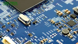
Every circuit board starts as a bare board—a foundation that defines whether your electronic product will succeed or fail. A bare pcb (before any components are placed) is the truest test of your manufacturing process and design discipline. At this pivotal phase, bare board testing ensures every conductive trace and via meets design specifications, and every test point is accessible for future testing or pcb assembly.
Bare board testing is widely utilized in critical industries such as consumer electronics and aerospace. This testing phase serves as a fundamental barrier against manufacturing defects. It also functions as a core tool for quality management, ensuring products meet predefined standards. The practice of testing supports compliance requirements, enabling companies to fulfill industry safety and environmental regulations. Its continuous implementation further optimizes production processes, enhancing overall manufacturing efficiency and reliability.
What is a Bare Board? Why Do We Use Bare Board Testing?

A bare board, also referred to as a bare PCB or an unpopulated printed circuit board, specifically denotes a circuit board that has been manufactured but has not yet been assembled with electronic components or connectors. This board exhibits a raw layered structure, composed of a substrate, copper traces, pads and vias. This structure is ready for integration into larger electronic assemblies. At this manufacturing stage, it is essential to rigorously verify the board’s electrical connections, trace integrity and insulation properties—a step that is of critical importance.
Why Use Bare Board Testing?
- Catch defects at the source: Faults in conductive pathways on a bare pcb can lead to catastrophic electronic failures if undetected before component assembly. Once components are placed, reworking a board is far more expensive, complex and can introduce new problems.
- Ensure proper electrical connections and isolation: Continuity and isolation checks guarantee current flows where intended—and nowhere else—before investment in component placement.
- Validate against design specifications: Every net and test point from your schematic is mapped onto actual copper—bare board testing cross-references these to guarantee every part aligns as planned.
- Process feedback: Discovering an open, short or layout mistake early in PCB manufacturing allows for rapid corrective action before full-scale production.
Core Principles of Bare Board Electrical Testing

Bare board electrical testing rests on two central concepts: ensuring continuity and isolation. These confirm each electrical pathway exists as designed and that unintended connections—short circuits—do not exist.
Continuity Testing
Ensures each trace, pad or via connects exactly as per schematic intent. If even a single trace is cut or a via is incomplete, the current cannot flow and the pcb fails at installation or in the field.
- Method uses: Robotic arms or a fixture to measure the resistance across each net. Ideal result: Low (milli-ohms).
Isolation Testing
Checks that adjacent nets or “two separate” electrical paths remain electrically isolated—meaning megohms or higher between connections.
- Prevents shorts, cross-talk or safety and functional safety threats.
- Vital for boards used in automotive, aerospace or medical device applications.
Electrical Parameter Tests
Advanced testing now covers:
- Kelvin Resistance Test: Ensures low-resistance, high-current paths are robust.
- Time Domain Reflectometer (TDR): Measures characteristic impedance for high-speed, high-frequency PCB boards.
- Hi-Pot and Insulation Resistance (IR): Simulates real-world voltage stress to confirm robust isolation.
Key Bare Board Testing Methods for PCB Boards
Two dominant technical approaches exist for bare board testing. Flying probe testing and bed-of-nails testing are widely adopted methods. Each demonstrates distinct technical advantages. They correspond to differentiated cost structures; each is suited for specific production scenarios.
Flying Probe Testing
The flying probe test method operates based on a robotic arm system. This system is equipped with two or more independent robotic arms. Each robotic arm carries movable probe mechanisms. Following preset programs, the probes sequentially make contact with test points on the surface of the printed circuit board. The number of test points can range from dozens to hundreds or even thousands.
- Main advantage of flying probe testing: Flexibility—no custom fixture needed. Ideal for prototypes, small-batch production and pcbs with frequent design changes.
- Advantage of flying probe testing: Capable of reaching high-density and BGA areas where traditional fixtures cannot.
- Testing process: Probes move across the bare pcb, touching pads and vias, measure the resistance or insulation between connections and collect data for each net pair.
Flying Probe vs Bed-of-Nails
| Criteria | Flying Probe | Bed-of-Nails |
| Setup Time | Minutes | Days/weeks |
| Fixture Cost | None | High (thousands of $) |
| Volume | Low, medium | Medium, high |
| Tests Accessible | Almost all | Sometimes limited by fixture / density |
| Speed (per board) | Slower | Ultra-fast |
| Adaptability to Design Changes | Immediate | Requires new fixture |
Bed-of-Nails Testing
This method uses an array of spring-loaded pins (“pogo pins”) pressed onto the fixture, making contact with all accessible test points in a single actuation.
- Uses a custom fixture designed for the PCB layout.
- Extremely rapid—tests thousands of test points in seconds, a huge asset for high-volume manufacturing.
- Bottleneck in high-volume manufacturing: The need for a new fixture with each PCB revision (can cost thousands for tooling and days to weeks to create).
From Prototyping to Mass Production: Building a Testing Strategy

Stage 1: Prototyping & Small-Batch Production
- Bare pcbs in this phase undergo flying probe testing to quickly surface open connections, shorts,or unintended resistance at any trace, pad or via.
- Minor design tweaks are common, so avoiding fixture costs is a priority.
- Benefit of bare board testing here: Reduced risk, rapid iteration.
Stage 2: Scaling Up
- For consistent designs, transition to bed-of-nails or a hybrid approach.
- Use lessons learned from early electrical test failures to improve future PCB layout and the manufacturing process.
Stage 3: Full-Scale Production
- High-quality pcbs require stringent, repeatable, and well-documented testing methods.
- The combined testing approach utilizes bed-of-nails testing for high-speed electrical testing. Automated optical inspection is applied for surface defect inspection. Flying probe testing addresses complex circuit networks or minor design revisions.
Industry Standards, High-Reliability and Compliance
The modern electronics manufacturing sector must comply with stringent technical standards. Regular audits are a fundamental requirement within the industry. The automotive, medical device, and aerospace industries impose heightened demands in this regard. Global PCB manufacturing standards provide clear specifications for production. Adherence to these standards not only ensures product acceptance by customers but also safeguards end-user safety.
Key Standards for Bare PCB Board Electrical Testing
- IPC-9252: Sets guidelines for electrical test methods, netlist coverage, test voltages and defect reporting for bare boards.
- IPC-6012: Specifies the quality, performance and acceptance criteria for rigid printed circuit boards – from trace width uniformity to insulation properties.
- ISO 26262: Functional safety for automotive electronics requires extremely rigorous electrical testing and a complete, traceable documentation system.
- IEC 60601-1, ISO 13485: Medical electronic products must undergo a series of mandatory tests. High-voltage testing validates the electrical safety strength of the product. Insulation testing ensures the isolation reliability of critical components.Traceability testing spans the entire production process to establish complete product documentation records.
- IPC-6012 Class 3: The defense and aerospace sectors adhere to the highest level of testing standards. These standards require testing to cover all network nodes on the circuit board. The production process must establish a complete technical documentation and recording system. Products also need to undergo repetitive testing and verification at specified intervals.
PCB Test Equipment: Technology, Automation & Methods

Modern bare board E-test systems leverage advanced robotics and precision instrumentation to transform test coverage from a bottleneck into a competitive advantage.
Flying Probe Testers
- Feature two robotic arms (sometimes more) with agile probes that move in a programmed sequence across the PCB substrate.
- Capable of executing Kelvin resistance measurements, IR and high-voltage tests on both sides of the board.
- Highly adaptable, with automatic test program generation from the design’s latest netlist.
Bed-of-Nails Testers
- Uses a custom fixture with an array of spring-loaded pins—each dedicated to a unique net or test location.
- Fixture is pressed onto the bare pcb board, instantly connecting to thousands of points and allowing simultaneous electrical test.
- Ideal for repeat runs, but fixture costs are only justified at volume.
Hybrid & Emerging Solutions
- Some test houses now deploy dual-mode systems: fast bed-of-nails for bulk checks and a flying probe for points inaccessible to the fixture—especially beneficial for high-density interconnect (HDI) designs.
- Next generation testers may leverage optical, capacitance or EM imaging for future, non-contact, high-speed inspection.
E-test Result Analysis and Root Cause Diagnosis
A failed electrical test does not represent a setback; it presents an opportunity for process improvement and yield optimization.
Common Failure Modes and Diagnostics
| Defect Type | Typical Root Cause | Diagnosis Approach | Example Remedy |
| Open Circuit | Over-etched trace, broken via | High resistance, “Current cannot flow” during continuity | Improve etch/drill |
| Short Circuit | Copper bridge, contamination | Low resistance between two separate nets on isolation test | AOI, clean-up, reroute |
| High DCR (Kelvin) | Thin copper, poor plating | Suspiciously high trace/via resistance | Tighten process |
| Impedance Mismatch | Trace geometry, substrate variance | TDR waveform deviation from design specification | Review stack-up |
Remember, the manufacturing process should always be adjusted after recurring trends in test failures. Effective teams combine these results with AOI and production data for comprehensive root cause analysis.
Benefits of Bare Board Testing: Cost, Quality and Yield
Every dollar spent on bare board testing returns multiples in reduced rework, higher yield and better field reliability.
Key Benefits
- Identify issues early and cheaply: It costs pennies to scrap a bare pcb board—once components are placed, that price skyrockets.
- Boost yield and reliability: E-test finds not only “hard” defects, but also creeping issues (microcracks, under-etched areas) invisible to the naked eye.
- Speed up assembly and QA: A passing E-test ensures the next stage—PCB assembly—can proceed without electrical surprises, reducing delays and warranty returns.
- Demonstrate compliance: Detailed E-test reports satisfy customer, auditor and market certification requirements, supporting bids for high-reliability and export contracts.
Challenges & Solutions in Bare Board Testing
Typical Challenges
- Dense or Miniaturized Designs: Fine-pitch BGAs, flex boards and HDI layouts make both visual and electrical access difficult.
- Fixture Costs: For bed-of-nails, even minor design changes may require a new fixture, adding thousands to project costs.
- Signal Integrity Checks: Complex products demand TDR and impedance validation, not just simple opens/shorts testing.
Solutions
- Use hybrid and flying probe testers for flexible access and adaptability to frequent design changes.
- Engage DFT and test engineers early in the design process to place accessible test points.
- Automate data analysis to spot process drifts and avoid unexpected scrap.
Where Bare Board E-test Delivers Value
The ROI on bare board electrical test is enormous wherever:
- Prototypes and NPI: Find design assumptions that don’t stand up in real manufacturing.
- Consumer Electronics: Mass-volume PCBs require cost-effective testing to preserve value across tens of thousands of units.
- Automotive & Aerospace: Lives and million-dollar assets depend on high-quality pcbs verified by regulated E-test standards.
- Medical Devices: Insulation (IR and hi-pot) checks ensure patient safety.
Best Practices, Advanced Tips, and Case Studies
- Automate every step: From test program creation (using IPC-D-356) to result reporting, automation reduces error, increases speed and saves money.
- Cross-validate with AOI: Combine electrical and visual inspection for a complete picture of PCB quality.
- Train for DFT: Empower designers to routinely consider test access and fixture compatibility.
Frequently Asked Questions (FAQs)
Why is bare board testing better than testing the assembled board?
Bare board testing lets you catch and correct critical defects while the cost of error is lowest—before expensive, sensitive electronic components are placed. This means higher yield and reliability at lower total cost.
What if my PCB design changes frequently?
The core design objective of flying probe testing is to achieve flexibility in testing solutions. This method eliminates the need to recreate physical fixtures. Adjustments to the testing process only require updating the test program scripts. This characteristic serves as a key advantage during the research and development phase. It is also well-suited for rapid prototyping. As a result, this technology represents an ideal testing solution for the initial stages of product development.
What’s the risk of skipping bare board E-test?
Extremely high: latent defects progress to the assembly stage, causing board or system failure, increased rework, lost customer trust, and, in regulated sectors, legal or recall liability.
How does using a custom fixture add value?
A custom fixture enables extremely quick bed-of-nails E-test for production runs, but only makes sense once your design is stable to avoid constant new fixture costs.
Conclusion: Building Quality into Every PCB Board
Bare board testing is not just a technical step—it’s an investment in your brand, your product and your future. Whether you’re developing next-gen wearables, failsafe automotive controls or life-saving medical equipment, using bare board testing ensures your pcb boards perform flawlessly at scale. By mastering both flying probe and bed-of-nails methods, you unlock cost-effective, agile and compliant manufacturing for every assembly stage—delivering high-quality PCBs to the world.Bare board testing is a fundamental technical procedure. This testing represents a strategic investment in brand value. It is directly linked to the long-term assurance of product quality. This technology also supports the sustainable development of enterprises. The development of various electronic products relies on the support of bare board testing. Whether for next-generation wearable devices, highly reliable automotive control systems or critical medical equipment, bare board testing ensures the stable performance of their circuit boards during mass production. Mastering both flying probe testing and bed-of-nails testing is essential. The application of these two technologies covers all assembly stages. Enterprises can thereby establish cost-controllable production processes. The manufacturing process also maintains flexible and efficient characteristics. The entire production system complies with industry standards and requirements. The ultimate goal is to consistently deliver high-quality circuit board products to the global market.