Introduction — Why PCB Design Matters for Beginners

As the backbone of modern electronics, printed circuit boards achieve the integration and miniaturization of complex circuits through precise wiring. The quality of their design and manufacturing directly determines the reliability of electronic devices. LHDT TECH believes that whether it is for electronics enthusiasts to start out or for engineers to develop professionally, it is crucial to have a systematic grasp of learning PCB design and understanding the process of creating PCBs is vital.
For this reason, we have specially step-by-step guide for beginners from to analyze the entire process of PCB from design to finished product from a systematic engineering perspective for you. This guide will gradually cover: design your first PCB, PCB layout and routing standards, key points of manufacturing processes, soldering and assembly techniques, and testing and verification methods. Whether you are looking to complete your simple LED circuit or develop reliable circuit boards for iot devices, LHDT TECH will provide you with a clear technical path and practical confidence through this comprehensive guide.
Understanding the Basics of PCB Design
Before delving into PCB design and layout, we emphasize that understanding the basic structure and functional principles of printed circuit boards is the core prerequisite for ensuring design feasibility and manufacturing reliability. PCB is not only the physical carrier of electronic components, but also a key architecture for achieving electrical interconnection and signal integrity. Mastering its basic composition and working mechanism will lay a solid technical foundation for subsequent design optimization, process selection and quality control.
What Is a PCB?

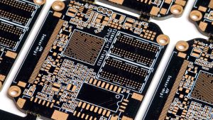
A PCB consists of:
- Copper traces connecting components instead of wires; these replace complex wiring almost in every modern device.
- An insulating substrate layer(most commonly FR-4).
- Pads to solder components.
- Solder mask to protect and insulate traces.
- Silkscreen on the top and bottom layers with text/graphics for assembly.
PCB technology significantly reduces the risks of misoperation and electrical connection in traditional wiring by achieving standardized and efficient assembly processes. Its high-density interconnection feature is the cornerstone for building compact and highly reliable circuit boards, and its application scope has extended from consumer-grade electronic products to industrial-grade smart devices.
Types of PCB Designs for Beginners
| PCB Type | Features | When to Use |
| Single-layer | One copper layer on the board | Very simple circuits |
| Double-layer | Copper on both sides | Standard hobbyist projects |
| Multi-layer | Separate internal power/ground planes for better performance | High-speed or dense board designs |
| Flexible PCBs | Bendable layers | Wearables, compact spaces |
| Rigid-Flex PCBs | Combination of rigid and flex layers | Advanced electronics requiring folding |
Essential PCB Design Terminology
- Schematic:A graphical representation of your circuit;
- PCB layout:Physical arrangement of components and conductive traces;
- Vias:Mini holes allowing connections between layers;
- Footprints:Physical layout of component pads on the PCB;
- Gerber files:The standard manufacturing files generated to fabricate your PCB;
- Bill of Materials (BOM):A list detailing every component needed.
Project Planning & Requirements Definition
Before creating a PCB, clear project goals and constraints must be outlined. This critical first step in any pcb design for beginners ensures straightforward pcb manufacturing and reliable operation.
Define Project Requirements
- What function will the circuit perform? (Signal processing, power control, sensors?)
- What are voltage, current, and thermal requirements?
- Environmental conditions: temperature range, moisture?
- Physical size limits—does your pcb board fit within a casing?
- How many layers does your design need? (Complex circuits usually require 4 or more)
- Production volume and cost constraints.
Budget Planning & Sourcing
- Select parts easily sourced with multiple suppliers, noting lead times.
- Plan budget for prototyping and eventual production.
- Account for tooling costs, assembly, and testing.
Gathering the Right Tools for PCB Design
Selecting the appropriate engineering software and toolchain is a key technical prerequisite for optimizing the overall process of designing a PCB and reducing the comprehensive complexity from layout to production file output.
Recommended PCB Design Software
| Software | Features | Cost/Access | Best For |
| EasyEDA | Web-based, large libraries, instant Gerber export | Free with premium options | Beginners & fast prototyping |
| KiCad | Advanced open-source, unlimited layers, active support | Fully free | Hobbyists & professionals |
| Eagle | Compact GUI, extensive libraries, Autodesk integration | Free tier available | Students & prosumers |
| Altium Designer | Professional-grade tool with simulation & team collaboration | Paid (expensive) | Industrial design |
Physical Tools for Assembly
- Anti-static protection system
- ESD protection workbench and grounding wristband: Ensure that the working environment complies with IEC 61340-5-1 standard to prevent static damage to sensitive components.
- Precision welding tools
- Adjustable temperature anti-static welding station: It is recommended to be equipped with a digital display temperature control system (temperature accuracy ±5°C) and multiple welding nozzles to meet the welding requirements of different package sizes.
- Welding auxiliary materials
- No-clean flux pen: Achieve precise coating and enhance soldering wettability.
- High-purity tin-absorbing braided tape: used for solder joint repair and removal of excess solder.
- Micro-assembly tools
- Anti-static precision tweezers set: including straight head and elbow models, meeting the mounting requirements of SMD components of 0201 and above sizes.
- Detection and testing instruments
- True RMS digital multimeter: used for measuring basic electrical parameters.
- (Advanced Configuration) Digital storage oscilloscope: Recommended models with a bandwidth of ≥100MHz are used for signal integrity analysis and fault diagnosis.
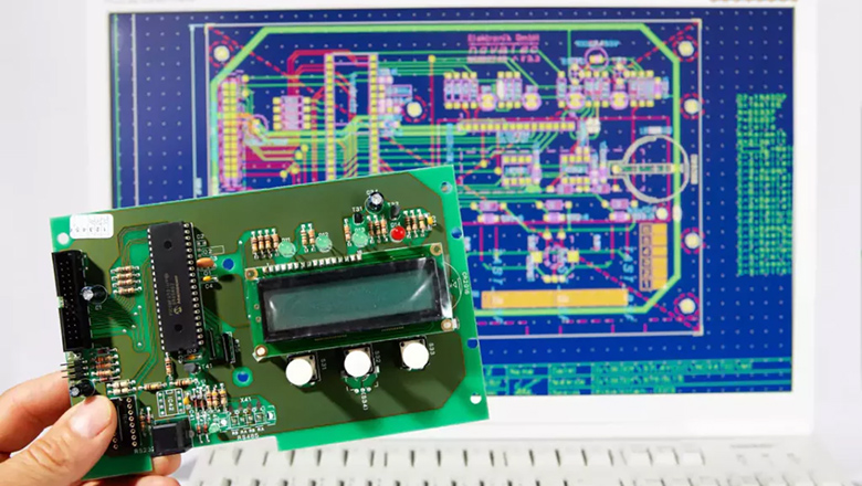
Schematic Capture & Library Preparation

A schematic diagram Starting with a clean and accurate schematic electrical connections is the foundation for ensuring seamless transformation and efficient connection from the logical definition stage to the physical layout stage in PCB design.
Capturing Your Circuit Schematic
- Draw components from verified component libraries.
- Connect nets logically—double-check no floating pins or conflicting connections.
- Add reference designators matching component names on BOM.
- Generate BOM (Bill of Materials) alongside schematic for procurement.
Verifying the Schematic
- Run Electrical Rule Checks (ERC) to identify logic/connection errors early.
- Use datasheets to confirm pin assignments and footprints.
Layer Stack-Up & Material Selection

Number of Layers
- For simple printed circuit board projects, 1-2 layers suffice.
- For dense circuit boards with high-speed signals or power distribution, 4+ layers improve noise reduction and routing.
Material Considerations
- FR-4 is standard for most hobby and commercial PCBs.
- Flexible materials like polyimide support bendable designs.
- Specialized substrates (Rogers, metal-core) address RF or thermal challenges.
Board Outline, Mechanical Interface & Placement Constraints
- Define your PCB outline to fit the enclosure perfectly.
- Ensure mounting holes align with mechanical supports.
- Respect design rules for clearances from board edges and mounting points.
- Use 3D preview to verify spacing, height, and mechanical fit.
Component Placement Strategies for Beginners
- Place connectors first at board edges for accessibility.
- Group related components to simplify routing.
- Place heat-generating components spaced apart with thermal reliefs.
- Align polarized components consistently for error-free soldering.
Routing, Trace Layout, and Power Planning
- Route wide traces for power—use online calculators or design software settings to determine appropriate trace width for current level.
- Avoid 90° bends; use 45° or rounded corners for better signal integrity.
- Use ground and power planes for low impedance, noise shielding, and thermal management.
- Manually route critical signals for better control over pcb layout.
Signal Integrity, Power Integrity, and Design for Manufactur ability
In the engineering philosophy of LHDT TECH, When designing a PCB must synergistically optimize signal integrity (SI) and power integrity (PI), which is the core foundation for ensuring the stable and reliable operation of your printed circuit board in complex practical working scenarios. Meanwhile, the systematic application of Design for Manufacturability (DFM) and Design for Testability (DFT) criteria can minimize pcb manufacturing process variations from the source, improve production yield, and provide guarantees for subsequent efficient assembly and precise testing, thereby achieving quality control throughout the product’s entire life cycle.
Signal Integrity (SI)
- Signal integrity is a key design criterion for ensuring that electrical signals maintain their timing, amplitude and waveform characteristics along the transmission path in high-speed digital and RF systemson pcb traces.
- Ensure signal integrity in the high-speed circuit design of high-speed serial link PCIe, USB 3.0+, Gigabit Ethernet, and memory interface (DDR4/5)
- Crosstalk suppression and wiring topology optimization strictly follow the 3W principle to reduce compatibility between adjacent signals. And for the key signal groups, differential pair routing and orthogonal layer routing strategies are adopted
- Impedance consistency control of transmission lines is implemented to carry out controlled impedance design for high-speed signals (such as DDR, PCIe, USB, etc.) and RF lines. The impedance control requirements and tolerance range are clearly marked in the PCB manufacturing documents.
- Add ground shields near critical signals to reduce noise and electromagnetic interference (EMI).
Power Integrity (PI)
- Clean and stable power is vital for reliable circuit boards.
- Use wide power and ground traces or solid copper planes for low resistance.
- Place decoupling capacitors close to IC power pins to filter voltage spikes.
- Route power supply traces with minimal loops to avoid noise injection.
Design for Manufacturability (DFM) and Design for Testability (DFT)
- Follow your pcb manufacturer’s DFM guidelines for minimum trace width, hole sizes, and spacing to avoid costly re-spins.
- Include ample test points on important signals for easy pcb testing during production.
- Keep surface-mount technology and through-hole components accessible for soldering and inspection.
- Submit complete and well-labeled design files along with other fabrication data.
Silkscreen, Markings, and Board Labeling
Adhering to professional make your pcb board layout can significantly enhance the engineering efficiency of PCBS during the assembly, debugging and maintenance stages. As a key carrier of visual information, the silk-screen layer should be systematically planned and include the following elements:
- Reference designators for all components (R1, C2, U1, etc.).
- Polarity marks on diodes, electrolytic capacitors, and LEDs.
- Board name, revision number, and date – critical for version control.
- Pin 1 indicators for ICs.
- Test point labels for quick identification.
Design Verification — DRC, ERC, and Simulation
Design Rule Check (DRC)
- Run DRC frequently during layout to ensure you meet design rules related to trace width, spacing, drill sizes, and clearances.
- Manufacturers provide tailored DRC rules to avoid issues during fabrication.
Electrical Rule Check (ERC)
- Validate your schematic with ERC to catch unconnected pins, floating nets, or short circuits before you proceed to pcb layout.
Simulation Tools
- Utilize simulation to predict power distribution and signal behavior.
- Tools like SPICE simulators within popular pcb design software help verify complex parts of your circuit.
Generating Manufacturing Files (Gerber, Drill, BOM)
The ultimate key technical link in the PCB design process is to generate and deliver standardized production document packages. This step is the core for accurately transmitting design data to manufacturing files, ensuring that all design intentions are completely and error-free converted into executable manufacturing instructions.
- Gerber files:Detailed layers of copper, solder mask, and silkscreen.
- Drill files:Location and size of holes and vias.
- BOM (Bill of Materials):Lists components and specifications.
- Pick-and-place files:Coordinates and orientations for assembly machines.
Always use your software’s design rule check and preview Gerbers before submission to your pcb manufacturer.
Soldering, Assembling, and Testing Your PCB

- Precision welding process control
- Using a digital display constant-temperature soldering station, an accurate temperature curve is set based on the alloy composition of the solder and the thermal sensitivity of the components to ensure the metallurgical quality of the solder joints and prevent thermal damage.
- It is step-by-step tutorial that operators receive standardized training based on the IPC-A-610 standard to systematically master the hierarchical soldering process of surface mount (SMD) and through-hole components.
- Hierarchical electrical verification process
- Basic layer: Use high-precision digital multimeters for connectivity tests and insulation resistance measurements to quickly eliminate basic faults such as short circuits and open circuits.
- Safe power-on: For the first power-on, a programmable DC power supply should be used, with voltage rise and current limit set (recommended ≤ 30% of the nominal value) to achieve active protection against potential overcurrent faults.
- Signal layer: For digital buses or sequential circuits, oscilloscopes are used for waveform and timing analysis. For complex protocols or multiple signals, it is recommended to use a logic analyzer or protocol analyzer for in-depth debugging.
FAQs — PCB Design for Beginners
Q: What software should a beginner use?
A:Before powering on, conduct a comprehensive connectivity test and insulation resistance measurement using a digital multimeter to eliminate basic hardware faults such as short circuits and open circuits.
Q: How many layers do I need for my PCB?
A:By using a programmable current-limiting power supply, the supply voltage is gradually increased in a stepwise manner, and the input current is closely monitored, thereby minimizing potential damage to the devices when a fault occurs.
Q: How do I test my first board?
A: On the basis of stable power supply, the tests of each functional module are carried out in sequence. For digital logic and timing issues, it is recommended to use an oscilloscope for waveform analysis. For complex bus communication, protocol layer debugging can be carried out with the help of a logic analyzer.
Q: What is a Gerber file?
A: It’s a manufacturing blueprint defining each layer of your pcb layout.
Conclusion — Take Your First Step from Idea to PCB in Hand!
This step-by-step guide to PCB design for beginners covered everything from basic theory to to production-ready pcb assembly. By now, you have the complete knowledge framework needed to start your pcb design software. The key to the next step lies in action: select the appropriate engineering toolchain, complete your first version of the circuit design, and after professional pcb designs verification, you can enter the production stage.
LHDT TECH always believes that whether it is the R&D team or independent developers, mastering the complete capabilities from design to manufacturing will open up a broad dimension of technological innovation for you. We look forward to becoming your key partner in transforming your creativity into reliable products with our professional technical accumulation and manufacturing capabilities.