What is PCB Drilling? Everything You Need to Know
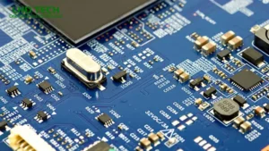
PCB drilling refers to the manufacturing process of precisely machining holes in printed circuit boards. This procedure serves the core function of interconnecting the circuit layers of the board. Its outcomes ensure both efficient electrical signal transmission and secure mechanical assembly of components. A thorough understanding of this process requires clarity on two key facts: drilling represents one of the highest-cost stages in PCB manufacturing and is also a production phase that demands extreme precision in processing. The quality of the drilled holes directly correlates with the board’s final performance, impacts the long-term reliability of solder joints and fundamentally determines theoverall quality level of the end product.
The precision design of PCB drilling processes is the prerequisite for achieving high-quality hole machining. These holes need to accurately form via hole structures to meet component assembly requirements and achieve mechanical mounting and positioning functions. In actual operations, it is necessary to employ a variety of drilling technologies and methods. The selection of each technology and method must comprehensively consider multiple factors such as the design requirements of the specific PCB, the physical properties of the circuit board materials used, the overall board thickness and the target aperture size.
Fundamentals of Drilling Techniques in PCB Manufacturing

Modern PCB manufacturing employs a variety of drilling techniques. The selection of drilling methods and the choice of drilling machines or bits must be based on the specific design requirements of each PCB and the characteristics of the substrate material. The fundamental knowledge to be mastered includes the following core aspects:
1. Mechanical Drilling

- Mechanical drilling is suitable for most through-holes, vias, and mounting features.
- Drill machines used in this process range from bench-top single-head to high-speed, multi-head CNC routers.
- Drill bits used in PCB drilling are commonly made from tungsten carbide for durability.
- Mechanical drilling creates accurate, repetitive holes for mid-to-large production and supports a variety of drill sizes.
2. Laser Drilling
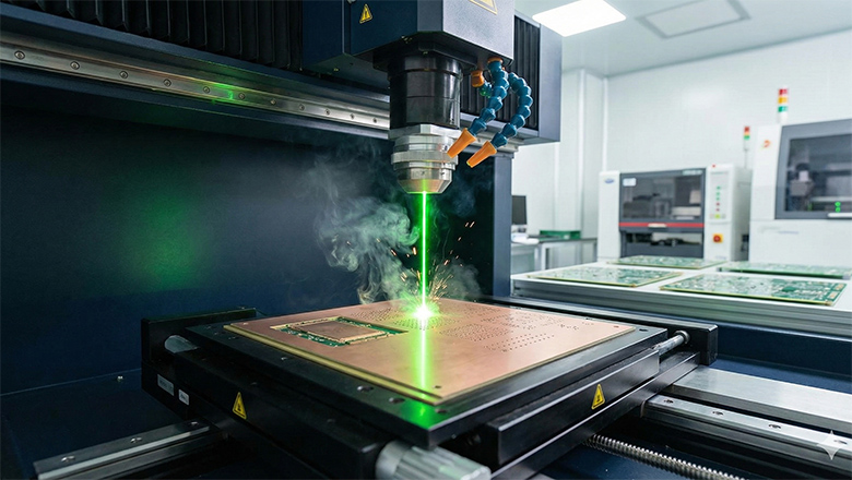
- Laser drilling uses a focused beam to ablate material, allowing for ultra-small holes and microvias.
- Laser drilling is a non-contact process, reducing mechanical stress and burring, making it ideal for HDI boards.
- Suitable for smaller holes plated with metal—as in high-density smartphone PCBs.
3. Vibration Drilling and Hybrid Methods
- Used for delicate materials or advanced stack-ups, often in medical or aerospace markets.
- Vibration adds oscillation to reduce burrs when drilling brittle or hard-to-machine substrates.
Quick Comparison Table: Drilling Technologies
| Drilling Technique | Holes Used To Drill | Advantages | Limitations |
| Mechanical Drilling | PTH, components, mounting | Cost-effective, versatile | Not suitable for ultra-small holes |
| Laser Drilling | Microvias, blind/buried | Precise holes, minimal damage | Higher equipment cost |
| Vibration/Hybrid | Special substrates | Lower burrs, improved hole quality | Specialized usage |
The PCB Drilling Process: Step-by-Step

To truly master PCB drilling technology, operators must be thoroughly familiar with the complete workflow from preliminary preparations through to final quality inspection. This step holds definitive significance in PCB manufacturing and its critical nature often leads to it being described as the “heartbeat” of the entire manufacturing process.
1. Preparation
- Generate a drill schedule specifying all hole and drill sizes, their types, locations and whether they are plated or not.
- Determine layers of the PCB, stack-up and registration holes.
- Select the suitable drill machine(mechanical, laser or hybrid) and assign drilling parameters like feed rate and spindle speed.
2. Drilling
- Drilling process must be carefully controlled to match PCB material and layer requirements.
- Drill depth is set based on whether you’re fabricating through-holes, blind vias, buried vias or controlled-depth features.
- Use bits used in PCB drilling(tungsten-carbide, polycrystalline diamond, coated) appropriate for the substrate and drill size.
3. Post-Drilling: Cleaning, Plating, and Inspection
- Remove burrs, dust, and debris—a necessity for copper plating of the interior of vias.
- Copper plating of the interior and barrel is done for PTH and vias, followed by surface finish for assembly.
- AOI(Automated Optical Inspection), electrical tests and X-ray checks ensure all holes in the PCB and drilled in the PCB meet tolerances.
Types of Holes in a Printed Circuit Board
Learning everything you need to know about the types of holes in a PCB is crucial for both design and manufacturing:
1. Plated Through Holes (PTH)
- These are holes in a printed circuit board plated with copper, essential for interconnecting layers and components.
2. Non-Plated Holes (NPTH)
- Used for mechanical mounting or tooling, non-plated holes don’t carry electrical signals but are critical for structure and assembly.
- Mounting holes, fiducials and tooling features rely on precise, accurate drilling.
3. Via Holes:
- Blind vias: Connect outer to one or more inner layers.
- Buried vias: Connect only internal PCB layers.
- Microvias: Ultra-small, suitable for finer pcb design in HDI boards.
- Through-hole vias: Span all layers, most common type.
4. Other Hole Features
- Slots/Oblong holes: For connectors or specialized components.
- Mouse bites: Used to help separate panels during depanelization.
Hole Types and Functionality
| Type | Purpose | Created by |
| Plated through-hole | Electrical + mechanical mounting | Mechanical/laser |
| Non-plated hole | Mechanical, alignment, mounting holes | Mechanical |
| Microvia | High-density, small form factor, BGA | Laser beam |
| Slot | Unusual parts, edge connectors, fuses | Router/drill |
Drilling Techniques: Mechanical and Laser Drilling
Drilling techniques selection can make or break PCB production:
Mechanical Drilling
- Used to drill holes in the PCB with spinning carbide bits.
- Mechanical drilling is suitable for most accurate PCB drilling needs in standard boards.
- Can drill precise holes but limited by bit diameter—smaller holes increase risk of bit breakage and manufacturing time.
Laser Drilling
- Laser drilling uses an intense laser beam to ablate material, allowing for high-density vias and tight pitches, especially needed for HDI applications.
- Laser drilling is a non-contact method, which makes it excellent for delicate layers and smaller holes with minimal substrate stress.
- Laser beam drilling offers unmatched flexibility for designers needing to create precise holes in advanced multi-layer boards. Since laser drilling is a non-contact method, it avoids mechanical stress and is ideal for drilling microvias—those incredibly small holes plated with metal for HDI and compact consumer electronics.
When to Use Each Drilling Technique:
- Mechanical drilling is suitable when your PCB design calls for larger, deeper or high-volume through-holes—common in traditional, industrial and power applications.
- Laser drilling is the process of choice for smaller holes, blind vias or stacked vias where precise drilling and minimal pad damage are paramount.
Key Factors to Consider in PCB Drilling

There are critical details to consider in PCB drilling that influence the success of both PCB manufacturing and end-use performance:
1. Drill-to-Copper Distance
- The gap between the hole and the nearest copper feature—this “drill to copper” spec is vital to avoid shorts, pad lift or breaking into traces during the drilling process.
2. Drill Sizes and Drill Depth
- In PCB manufacturing, operators must select drill bit specifications based on the pad and via dimension requirements specified in the design documents, while also taking into account the tolerance range in the production process.
- Drill depth determines whether you’re creating through-holes, blind vias or controlled-depth features for back drilling.
3. PCB Material and Stacks
- The hardness and composition of the PCB material, including glass content and copper thickness, dictate drilling speed, feed rate and bit type.
- High-Tg or metal-backed PCBs require adjusted drilling parameters and bits used in PCB drilling.
4. PCB Layers and Registration
- High-layer-count PCBs demand accurate registration and sometimes the use of X-ray guided drilling machines to align with internal reference points for holes drilled in the PCB.
5. Drilling Parameters
- In PCB drilling operations, feed rate, spindle speed, dwell time and cooling/lubrication effectiveness are key processing parameters. The settings of these parameters jointly determine the actual service life of the drill bit and the quality of the resulting PCB holes.
- Automated drilling machines and CNC systems monitor these parameters in real time for consistent performance.
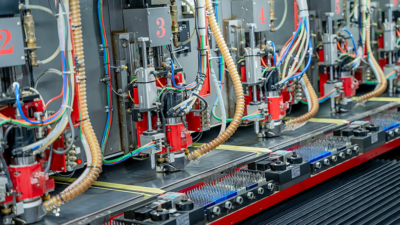
Automated Drilling Machines: Efficiency and Accuracy
Automated drilling machines—including multi-head CNCs and high-speed routers—enable rapid, accurate drilling for today’s demanding boards. These systems are a vital part of professional PCB fabrication and are used to drill holes of all types and sizes.
How Automated Drilling Machines Work
- Tool Changers: Allow for seamless transition between different drill sizes, optimizing time and reducing errors.
- Vision & Registration Systems: Real-time cameras and fiducial detection auto-correct for stack or panel misalignment, ensuring accurate PCB drilling and consistent quality.
- Data Logging: Every drilled hole is tracked for position, diameter and bit wear, providing feedback to master PCB drilling processes.
Advantages:
- High accuracy and repeatability for multiple boards.
- Shorter drilling time for large production runs.
- Ability to create holes on the PCB with complex layer stacks accurately every time.
PCB Design Guidelines for Master PCB Drilling
Proper PCB design is essential for reliable, cost-effective drilling and assembly.
Design Steps for Accurate PCB Drilling
- Standardize drill sizes: Minimize unique hole counts to reduce tool changes and manufacturing costs.
- Specify PTH vs NPTH clearly in your design files.
- Maintain proper drill-to-copper distance: This avoids electrical shorts and increases manufacturing yield.
- Leave proper annular rings: Ensure sufficient copper around every plated through-hole for a robust mechanical bond.
- Use test coupons and reference holes for quality control during high-reliability runs.
- Accommodate drilling tolerances: Factor in allowed diameter and location drift based on your PCB manufacturer’s printed circuit board capabilities.
DFM Best Practices
- Engage your PCB manufacturer early to review the drill table, layer stack and materials.
- Assess the drilling process for features like mounting holes, back-drilled stubs and high-aspect-ratio (deep) vias.
- Balance density and reliability: Pursuing smaller hole diameters increases both cost and risk. They should only be used where they provide genuine design value.
LHD TECH’S Tips for Accurate PCB Drilling and Professional Results

The execution phase of the PCB drilling process must pay full and thorough attention to every detail in the drilling procedure to achieve finished product quality that meets professional processing standards and produce high-quality printed circuit boards.
- Always specify the depth of the drill bit for controlled-depth features to avoid damaging other layers of the PCB.
- Use automated drilling machines for large batches to maintain repeatability and reduce operator error.
- Choose drilling techniques that best suit your application—mechanical for high-volume, robust, cost-effective holes; laser for microvias and fine features.
- Conduct routine maintenance on your drill machine and regularly replace bits used in PCB drilling.
- Confirm that holes in PCBs are free from burrs, resin smear or copper pull-away.
- For mission-critical boards, demand cross-sectional analysis of vias for copper plating quality.
- If your board has PCB layers of different materials, consult your manufacturer about thermal expansion and registration strategies—they affect drill accuracy.
Quality Control: Ensuring the Best in PCB Drilling
PCB quality depends on stringent inspection before, during and after drilling:
- AOI and Visual Inspection: Find miss-drilled, under drilled or oversized holes.
- Electrical Testing: Bed-of-nails and flying probe testers verify every plated via for continuity.
- X-ray and Microsection: Essential for multi-layer HDI boards to confirm hole registration and copper plating of the interior.
- SPC Data Tracking: Drill machines log every hit, noting wear and performance—this prevents defective boards and optimizes the drilling process.
Professional PCB manufacturers will provide inspection reports, drill hit counts and verification data to prove quality.
Expert FAQs: Everything You Need to Know About PCB Drilling
Q: Why is drilling one of the most expensive steps in PCB manufacturing?
A: Drilling time, number of bits used, need for precise holes across many types/layers and tool change/inspection all add up to significant cost.
Q: What should I know about PCB drilling for multilayer PCBs?
A: Registration and depth control are paramount. X-ray-guided automated drilling, correct drill sizes and appropriate techniques (mechanical or laser) ensure reliable hole placement and copper plating even in high layer-count designs.
Q: Does the process of creating holes affect signal performance?
A: Yes. Improper drill to copper clearances, misalignment or poor plating can cause high-frequency losses, EMI or long-term reliability issues. For high-speed, always ask for stub removal (backdrilling) and high-quality via filling.
Q: How is drill to copper defined and why does it matter?
A: It’s the minimum distance from the edge of a drilled hole to the nearest copper feature. Too little space leads to broken rings, shorts or unreliable solder joints—check your fab’s recommended value during the design phase.
Q: Are smaller holes or microvias difficult to plate?
A: Yes, smaller and deeper holes—especially those drilled by laser—require pulse plating and careful prep to ensure copper plating of the interior is sufficient for electrical and mechanical reliability.
Conclusion: Master PCB Drilling for High Performance
Everything you need to know about PCB drilling starts with understanding how the drilling process impacts PCB performance, manufacturing yield and final reliability. From choosing the right drill machine, bit and technique, to mastering drill sizes, material stack up and PCB design rules, success is in the details.
To master PCB drilling, remember:
- Choose the right drilling technique for each feature (mechanical, laser or hybrid).
- Specify accurate PCB drilling schedules in your design files and communicate them clearly to your PCB manufacturer.
- Consider in PCB drilling the balance between density, reliability and manufacturability.
- Always verify quality through optical, X-ray and electrical inspection at every production stage.
- Work with a manufacturer who has the expertise, equipment and commitment to help you meet the specific requirements of the PCB design and application.
For reliable high-performance printed circuit boards, drilling is a critical step that cannot be overlooked. Leverage these guidelines, work with professional PCB partners and you will master the art and science of accurate, high-quality PCB drilling.