Introduction
The manufacturing of printed circuit boards (PCBs) and the electronics industry impose stringent requirements on design procedures and key process points. Signal integrity is critical to data transmission quality, modular upgradability affects equipment expansion capability, and long-term reliability under harsh environments determines product service life.In modern electronic devices, PCB gold fingers—responsible for electrical connection, power delivery, and high-speed data transmission—serve as core components. A thorough understanding of PCB gold fingers requires mastery of three aspects: design purpose defines their structural features, the critical role of reliable connectors influences system stability, and the sophisticated electroplating processes behind their high performance involve materials science and chemical deposition technologies.
Whether it’s a server module that needs to be swapped without a single lost packet, or a medical device that must remain corrosion-resistant and reliable, pcb gold fingers are the gold-plated edge connectors at the heart of these innovations. In this guide, we’ll dive deep into the gold finger pcb, covering the gold finger plating process, thickness, types of gold fingers, hard gold vs ENIG, what you absolutely need to know about PCB manufacturing, and the secrets behind high-quality PCB gold finger plating.
Engineers and designers prioritize reliability, durability and signal stability when developing products. The technical characteristics of PCB gold fingers precisely meet these requirements. This article provides a detailed analysis of PCB gold plating technology while introducing key aspects of the PCB design and manufacturing process. Gold plating thickness affects insertion cycles and contact resistance, with electroless nickel immersion gold and electroplated hard gold processes each suited to different applications. The design phase requires consideration of parameters such as gold finger chamfer angles, trace length control, and spacing between adjacent fingers, while the manufacturing process involves control of plating uniformity and surface finish quality inspection.
What Are PCB Gold Fingers?

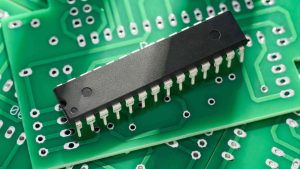
PCB gold fingers are designed at the edge of the circuit board, utilizing gold plating technology to form connection contacts. These gold finger contacts feature an elongated shape, yet their functional role is far from simple. The gold finger structure supports modular design and serves as a core connection component. The quality of the gold finger directly reflects the engineering level of PCB assembly, with gold layer thickness affecting contact resistance, surface hardness determining insertion cycles, and edge flatness relating to signal transmission quality.
Gold fingers provide the connection function between a PCB and an interface. This structure ensures stable and continuous transmission of electrical signals between the board and components. Observing the edge of a circuit board reveals finger-shaped pads fabricated using gold plating technology. These pads feature a finger-like shape and are designed for insertion into corresponding slots or connectors. Practical application scenarios include RAM modules, PCIe graphics cards, medical device plug-ins and other electronic assemblies requiring frequent insertion and removal.
Key points about gold finger PCBs:
- Gold fingers are the gold-plated contacts that interface with an external connector.
- Gold fingers are processed using specialized plating techniques. These techniques include electroplated hard gold, electroless nickel immersion gold (ENIG) and other gold surface finishing methods. Electroplated hard gold enhances the wear resistance of contacts, ENIG improves soldering reliability and other gold finishes cater to specific application requirements. Each plating technology has particular technical parameter control requirements.
- Their locations at the edge of the circuit board are designed to facilitate insertion into a slot while ensuring reliable electrical connections.
- The design parameters of the gold finger—thickness, surface finish, and design rules—must all comply with strict industry specifications. These requirements ensure connection reliability, particularly in scenarios involving frequent insertion and removal or high-speed transmission, guaranteeing signal integrity and long service life.
Fingers on a PCB are not just another set of pads—they’re engineered to maximize signal integrity, minimize oxidation and withstand the mechanical wear of thousands of insertion/removal cycles.
Why Gold Finger Plating is Essential

You may wonder, “why plate PCB edge connectors at all?” The answer lies in the environments and use-cases these PCB edge fingers endure:
- The application of gold plating leads to vanishingly small contact resistance. This characteristic ensures reliable transmission: signals are delivered rapidly and power is transferred with minimal loss.
- Gold possesses strong resistance to oxidation and corrosion, a characteristic that distinguishes it from most other metals. This property forms the foundation for maintaining consistently stable connections in connectors throughout their long-term use.
- The plating process gives a robust, durable finish, especially if you’re using hard gold. This is vital for high-cycle connectors like expansion cards, network line cards or military modules.
- PCB gold fingers require this unique finish to perform seamlessly in industries like industrial controls, medical electronics, defense, telecommunications and wherever uptime is critical.
Learn about PCB gold fingers and their plating process, and you’ll realize: cutting costs here puts your entire board at risk of failure. Because gold is expensive, PCB gold finger plating is only applied where needed—the rest of the PCB surface will use a more economical finish, like HASL or OSP.
Types of Gold & Gold Finishes
There are various methods available for plating gold onto PCB gold fingers. Differences in the gold layer’s fabrication process directly affect multiple aspects of the circuit board, including its service life, electrical performance and wear resistance.
- Hard Gold (Electroplated Hard Gold): A layer of gold, alloyed with cobalt or nickel, is electroplated onto the nickel barrier. These “hard gold” finishes are engineered for thousands of insertion/removal cycles in demanding applications—think of industrial slot cards or gaming GPUs.
- ENIG (Electroless Nickel Immersion Gold): The ENIG process deposits a very thin, high-purity gold layer onto the nickel surface through chemical immersion. This method achieves exceptional surface flatness and is primarily intended for SMD pads or gold finger scenarios designed for a lower number of insertion cycles.
- Soft Gold: Pure gold electroplated without alloying. Soft gold is reserved for wire bonding pads and niche applications, not finger connectors.
- ENEPIG: The ENEPIG process involves inserting a palladium layer as a diffusion barrier between the electroless nickel layer and the immersion gold layer. This high-performance surface finish is typically specified for connectors requiring high reliability or those involving mixed technology assembly.
When specifying a gold finger PCB, the types of gold and plating method—hard gold, soft gold, ENIG, ENEPIG—depend on signal needs, connector wear and project budget.
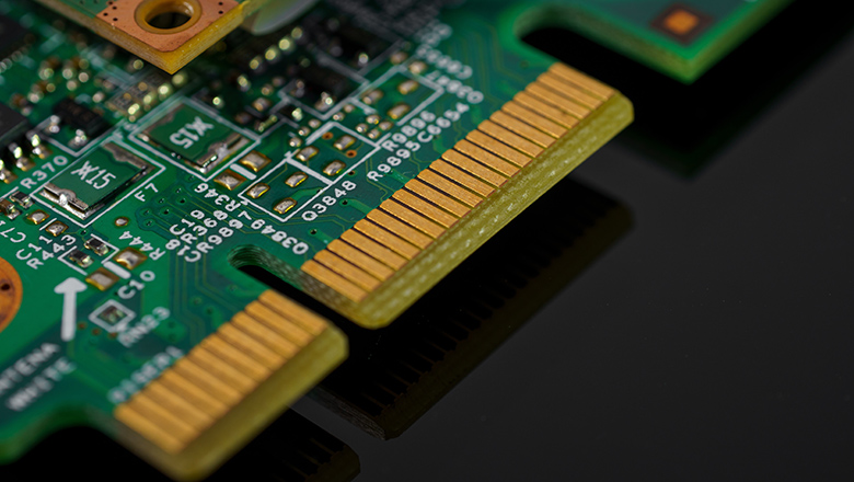
PCB Gold Fingers: Construction and Plating Process
The Anatomy of Reliable Gold Fingers
Every pcb gold finger is engineered from the inside out:
- Copper Layer:Forms the conductive backbone connecting to the rest of the PCB.
- Nickel Barrier:A carefully applied barrier plate of 100–150 µin, crucial for preventing copper migration into the gold and enhancing wear resistance.
- Gold Finger Plating:The final gold layer (thickness typically 10–50 µin for hard gold) is applied via electroplated gold plating process or the ENIG plating process.
The PCB Gold Finger Plating Process
PCB gold finger plating process steps:
- Edge Preparation:The edges of a printed circuit are precisely routed and cleaned for adhesion.
- Nickel Plating:The copper is first plated with a nickel barrier layer to ensure hardness and block copper diffusion.
- Gold Plating:Pure or alloyed gold is deposited through either hard gold plating (electroplated over nickel) or the ENIG process (immersion gold).
- Beveling:The edge or chamfer of the PCB is often beveled to make it easier to insert the PCB into a slot/connector and prevent finger damage.
- QA Inspection:XRF and other inspections confirm the thickness of the gold, adhesion, and absence of oxidation or impurities.
Why care about these complexities of PCB design?
Because a failure in the gold finger plating process leads directly to field failures, signal dropouts or even burned connectors.
Types of Gold Fingers & Gold Finishes
Gold fingers are not all created the same—design rules and usage vary:
- Standard (Flush) Gold Fingers:Evenly spaced, right at the PCB edge—a classic for modular design.
- Uneven or Staggered Gold Fingers:Designed so certain pins connect/disconnect first for power-up sequencing or ESD protection.
- Segmented Fingers:Separated groups of fingers for different voltages or signal grounds, improving signal quality in mixed-technology environments.
Which Gold Finger Plating Types Match Which Application?
| Finger Style | Typical Gold Type | Plating Process | Use Case |
| Standard (Flush) | Electroplated Hard Gold | Electroplating | RAM, PCIe, Industrial Backplanes |
| Uneven/Staggered | Hard Gold or ENIG | Electroplating/ENIG | Hot-swap, Test Modules |
| Segmented | Hard Gold with ENIG Mix | Hybrid | High-frequency, Mixed Analog |
| Fine-Pitch/Narrow Gold | ENIG or Thin Hard Gold | ENIG/Electroplating | M.2, SSDs, micro connectors |
| High-Power/Current Fingers | Thick Hard Gold | Electroplating | Power distribution, edge fingers |
| Rigid & Ceramic PCBs | Hard Gold/ENIG/ENEPIG | Varies | High-temp, industrial, or ceramic PCB |
Hard Gold vs ENIG: Choosing the Right Gold Finger Plating
If you want to learn about PCB gold fingers, you must understand the difference between hard gold vs ENIG:
Hard Gold Plating
- Electroplated hard gold is gold alloyed with cobalt or nickel, noted for remarkable wear resistance and low contact resistance.
- This gold finger plating process produces a robust, non-porous layer, making it ideal for edge fingers that will endure thousands of connection cycles—the “workhorse” of the connector world.
- Hard gold offers optimal stability for high-speed, high-power connectors on all types of gold finger PCBs, including ceramic PCBs for advanced industrial or aerospace applications.
ENIG Plating
- The ENIG (Electroless Nickel Immersion Gold) gold plating process offers a thin, ultra-flat pure gold layer over a nickel barrier. It is favored where connector wear isn’t extreme, but signal planarity and solderability are key (e.g., hybrid connector/SMD pad boards).
- ENIG is typically more affordable and uses less gold, but isn’t as durable in high-wear edge of printed circuit boards applications.
Design Considerations and Industry Standards
High-quality PCB designs consider everything from plating process to mechanical fit and thickness:
- Plating Process Selection:The right plating process (hard gold vs ENIG, soft gold for special use) is chosen based on expected usage cycles and electrical requirements. Only plate the gold fingers, not the rest of the PCB surface, to control costs.
- Edge of the PCB Preparation:The edge of the printed circuit board needs a precise, burr-free finish to maximize contact and reduce insertion friction.
- Beveling:A 30° or 45° bevel angle at the connector end makes it easier to insert the PCB into a slot, protects the rest of the PCB and ensures even plating.
- Thickness Control:Strict QA ensures a uniform and adequate gold finger thickness. Industry standards such as IPC-2221, IPC-A-600 and IPC-6012 must be followed.
- Copper pull-back and solder mask clearance:Ensure that no copper or solder mask interferes with the gold finger region to avoid oxidation or connectivity issues.
- Connector slot compatibility:The finger layout, spacing, and width must perfectly pair with your chosen connector.
The Role of Gold Finger Thickness
The thickness of the gold on your PCB fingers is a spec you can’t overlook if you want reliable gold connections.
Typical Guidelines:
- 30–50 µin for most industrial and computing connectors
- Up to 100 µin for aerospace or military
- <5 µin for ENIG or soft gold applications
Gold finger thickness impacts:
- Insertion/removal cycle resistance
- Protection against oxidation/corrosion (longer lifespan)
- The overall performance and reliability of the connector
If gold fingers must withstand extensive wear, specify thicker plating. Don’t let your fabricator choose a “default” that’s too thin—gold finger failure due to inadequate thickness is a leading cause of intermittent PCB connector problems.
Applications: Where PCB Gold Fingers Are Used
Let’s explore exactly where PCB gold fingers are used and why they’re specified:
- RAM Modules and GPUs:Those narrow gold fingers at the edge of your memory or graphics card are hard gold plated to survive thousands of swaps and support high-speed data transfer.
- PCIe, M.2, Expansion Cards:Every time you slot a PCB into a server, gaming motherboard, or networking switch, the fingers on that PCB have to make flawless electrical contact.
- Backplane Systems and Modular Industrial Controls:Hard gold finger plating is a must—system uptime depends on the durability of those edge fingers.
- Medical and Test Equipment:Gold plating prevents oxidation and micro-corrosion in environments exposed to chemicals, sweat, or repeated plug/unplug cycles.
- Wearable Tech, Automotive, Aerospace, Power Distribution, Ceramic PCB:Only gold can handle the unique combinations of vibration, heat, humidity, and frequent servicing in these environments.
Common Problems With Gold Finger PCBs

Poor PCB manufacturing or cost-cutting on gold finger plating can create costly headaches:
- Gold Wear-Through/Oxidation:If your thickness is insufficient, or your plating process is defective, the copper or nickel beneath will oxidize—causing signal loss.
- Contamination:Oils, dust or solder mask on gold fingers increases contact resistance. Cleanliness during and after PCB assembly is key.
- Bad Beveling/Inconsistent Plating:Rough edges or uneven gold finger plating makes it harder to insert the PCB or damages connector contacts.
- Plating Delamination:Inadequate surface prep or poor gold finger plating process causes the layer of gold to separate from the nickel or copper base.
The Future of Gold Finger PCB Manufacturing
Emerging trends in pcb design and manufacturing mean:
- Automated gold thickness control and AI-based inspection are raising high-quality PCB.
- New gold alloys may support even more environmentally robust finishes for edge fingers.
- Sustainability efforts are focused on recycling gold from PCBs and reusing “rest of the PCB” materials, reducing both cost and environmental footprint.
- Advanced ceramic PCB and rigid-flexible PCBs are beginning to use gold finger plating for challenging applications—further proof that gold fingers are essential to tomorrow’s electronics.
FAQs: What You Need To Know About PCB Gold Fingers
How do I know what gold finger thickness is right?
Follow IPC-2221 or ask an experienced PCB assembly house—don’t just pick the cheapest option. The cycle life and quality of your finished connectors depend on it!
Do all gold fingers use pure gold?
No. Hard gold is alloyed (often with cobalt or nickel) for wear resistance, while soft gold (nearly pure) is for bonding or ENIG is selected for low-wear, high-solderability.
Can gold finger plating be used on the rest of the PCB?
Rarely—gold is expensive and only edge fingers need this durability. The rest of the PCB surface usually gets HASL, OSP or other finishes.
Is there a minimum width for gold fingers?
Yes, dictated by connector type and industry standards—don’t design them too narrow or you risk poor electrical connection and increased wear.
Can ceramic PCB use gold finger plating?
Absolutely. The plating process is different, but gold fingers are ideal for high-reliability, high-temperature board edges.
What is the biggest mistake with gold finger PCBs?
Failing to specify the right plating process, thickness or not following design considerations—leading to unreliable gold contacts.
Conclusion
In summary, if you want the perfect balance of modularity, reliability, connector longevity and signal purity, gold fingers are the gold-plated solution you need for your PCB. They require attention to detail—from the nickel plating barrier, gold finger thickness, industry standards for beveling, to the precise type of gold finish. Never compromise on gold finger plating process or use short-cuts; high-quality PCB manufacturing means the difference between your product’s reputation for reliability or a future filled with costly RMAs and downtime. The edges of a printed circuit board bear a heavy burden: every insert and removal, every burst of power and data, relies directly on the quality of your gold finger PCB.
To ensure your design stands out as a high-quality PCB, pay close attention to the following design considerations:
- Always use hard gold plating for edge fingers on PCBs subjected to regular cycles, remembering that the right thickness of the gold is non-negotiable in critical applications.
- For cost-saving, apply gold finger plating only to the parts of the PCB that require gold—namely the edge fingers—while using alternative surface finishes for the rest of the PCB surface.
- Specify the plating process, desired gold finger thickness, and connector requirements clearly in your PCB manufacturing documentation.
- If you’re exploring new form factors, like rigid-flex boards or ceramic PCB substrates, consult your manufacturer about appropriate gold finishes, as the plating process can differ.
- Diligently follow industry standards (such as IPC-2221 and IPC-6012) and thoroughly review your fabricator’s plating and inspection reports.
Gold fingers are the gold-plated, high-durability edge connectors—the hands that allow your board to communicate, upgrade and survive even in the toughest use-case.