
Introduction: The Role of the PCB Laboratory

The PCB laboratory is at the heart of the electronics industry’s relentless drive for quality, performance and safety. The work carried out in this lab—testing and analyzing various types of printed circuit boards—directly determines the reliability of the final products. The manufacturing process of electronic circuit boards is complex and requires high precision, demanding advanced testing and analysis at every stage. Every board, from medical equipment to automotive systems, must pass rigorous inspection and analysis to meet the highest standards.
Every circuit board must undergo a complete PCB laboratory testing process.This process verifies product compliance with IPC standards, ensures firm and reliable solder joints, and maintains stable circuit functionality.The testing scope of modern laboratories includes copper thickness measurement, component placement inspection, solder integrity analysis, and electrical signal behavior testing.These test data help engineers validate the feasibility of the design and prevent product failures in actual operation.
Foundations of a World-Class PCB Laboratory

A world-class PCB laboratory is equipped with proper equipment. The lab environment is strictly controlled and managed by professionals. The source of every material and the execution of every process have been recorded and meticulously examined.
Key Capabilities & Expertise You’ll Find in Leading PCB Laboratories:
- Environmental controls (static, temperature, humidity) essential for handling sensitive electronic circuits
- Segregated process zones: raw material intake, chemical processing, assembly and testing
- Magnification tools for thorough board inspection and analysis
- Advanced equipment for test, from AOI to X-ray and ICT
- Documented compliance with international standards such as IPC, ISO and CNAS
Building Your PCB Laboratory: Facility, Equipment and Standards
A high-tech PCB laboratory facility requires careful planning regarding layout, environmental requirements, process workflow and test equipment selection.
LHDPCB’S Essential Steps in PCB Laboratory Construction

1. Site Selection and Layout
- Choose a clean, low-vibration facility.
- Plan logical flow: from circuit board material storage to assembly lines, test and shipping.
2. Environmental Controls
- Install climate control and anti-static measures for sensitive electronic circuit boards.
3. Segregated Work Zones
- Isolate chemical handling from soldering and inspection.
- Designate dedicated assembly and test areas to avoid cross-contamination.
4. Critical Equipment Acquisition
- Optical microscopes for detailed pcb analysis and magnification.
- AOI systems and X-ray machines for non-destructive inspection.
- Flying probe testers and in-circuit testers for comprehensive electric function verification.
- Burn-in racks, vibration tables and environmental chambers for reliability tests.
5. Standards and Certification
- Seek IPC and ISO9001 certification for your electronic laboratory.
- Follow standard operating procedures for each step.
| PCB Laboratory Step | Purpose | Tool/Equipment Example |
| PCB Material Storage | Environmental protection | ESD Shelving, Humidity Meters |
| PCB Assembly | Population of pins/components on boards | Pick-and-place, soldering |
| Solder Joint Inspection | Evaluate joint quality | AOI, X-ray, Magnification |
| Circuit Board Functional Test | Ensure correct electronic operation | ICT, Flying Probe Testers |
| Failure Analysis | Identify root causes | Cross-section, SEM |
Workflow in PCB Laboratories: From Raw Material to Finished Board

The workflow in a PCB laboratory consists of multiple precision steps. These steps are closely connected, with each one executed in accordance with standard operating procedures and IPC standards. The entire process begins with the input of raw materials, such as copper-clad laminates, and ends with the output of printed circuit boards. The final products are verified and reliable, with the whole process remaining under strict control throughout.
LHD PCB Step-by-Step PCB Laboratory Process
- Material Preparation: Inspectors perform visual inspection and dimensional measurement on each PCB blank.The inspection focuses primarily on detecting surface defects on the board, while the measurement covers board thickness data and surface conditions.
- Imaging and Print Transfer: Photolithography process is responsible for transferring the circuit pattern onto the PCB blank.Through the use of photosensitive materials and the exposure procedure, this step fully reproduces and accurately positions the designed pattern onto the board surface.
- Component Mounting: Operators perform mounting and soldering on each pin or chip.These operations can be completed either manually or with the help of automated equipment.
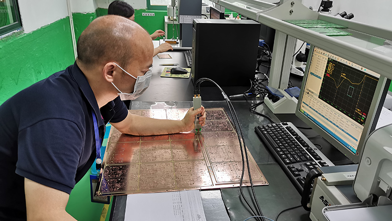
- Inspection and Test: Automatic Optical Inspection (AOI) equipment scans the board surface to detect issues such as component misalignment and bridging.Operators also use magnification tools to check the solder joint fill condition and verify the presence of components one by one.
- Functional and Electrical Testing: Employ flying probe, in-circuit test (ICT), and impedance analysis for the finished electronic circuit board.
- Lab Analysis and Documentation: Record each measurement, scan key assemblies, and log data for traceability.
LHD Essential PCB Test and Inspection Methods
The testing process involves a combination of methods. Operators use these methods to identify potential issues one by one in various parts of the printed circuit boards during production.
Non-Destructive Test Methods
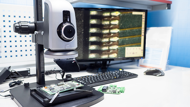
- Visual and Magnification-Based Inspection: Detect macro and micro defects on the circuit board surface or in solder joints.
- Automated Optical Inspection (AOI): High-speed, automated scanning for defects against the design.
- X-ray Inspection: Identify hidden problems inside multi-layer board stacks (e.g., inadequate solder, voids, pin misalignment).
- Electrical Measurement: Use ICT or flying probe to ensure every circuit path and pin functions as designed.
Destructive Analysis Techniques
- Microsectioning: Cut and polish cross-sections for in-depth material and failure analysis.
- Tensile/Solder Pull Tests: Inspectors measure the mechanical strength of solder joints.This data is used to evaluate solder joint reliability, which is especially critical for electronic devices in the automotive and aerospace fields.
Advanced Analysis
- Thermal Imaging: Finds overheating areas on active circuit boards.
- Chemical Analysis: Confirms composition of solder, copper plating or other materials (important for RoHS or export standards).
Failure Analysis and Improvement in PCB Laboratory Service
No matter how advanced your design or facility, some circuit board failures are inevitable. The difference is how quickly and thoroughly they are identified, analyzed and prevented from recurring.
Steps in Advanced PCB Failure Analysis
- Symptom Recording: Note exactly how/when the failure appeared.
- Physical Inspection: Use magnification, X-ray and AOI to search for visible faults.
- Electrical Testing: Check continuity of each circuit (especially critical pins) and perform parameter measurement.
- Destructive Analysis: Employ microsectioning for deep investigation into board construction issues.
- Root Cause Documentation: Summarize findings and suggest corrective actions—be it material change, assembly fix or redesign.
Customer-Specific Testing, Standard Compliance and Traceability
PCB laboratory services in different fields need to be tailored based on specific requirements. Aerospace, medical equipment, and telecom base stations have distinctly different requirements for circuit boards compared to ordinary consumer electronics. Clients propose customized testing plans according to their respective industries. These plans follow specific standards and ensure full traceability from equipment and batches to operational records.
Working With Standards (IPC, ISO, Industry-Specific)
- The IPC standards include a number of specifications, such as IPC‑A‑600 Acceptability of Printed Boards and IPC‑6012 Specification for Qualification and Performance of Rigid Printed Boards. These documents provide the fundamental reference requirements.Top laboratories go beyond these standards by also implementing the ISO 9001 quality management system and the ISO 17025 requirements for laboratory competence accreditation, while following industry‑specific specifications.
- All tests, inspections, and even staff training are logged per standard operating procedure for full audit readiness.
Product Traceability
- The production process assigns a unique code to each PCB. This code can take the form of a barcode, data matrix code or RFID tag. From the input of base materials to the output of the finished circuit board, the code accompanies the board throughout the entire process for lifecycle tracking purposes.
- All measurements, test outcomes, and even operator/inspector IDs are linked to the specific serial number in the laboratory information system.
- This enables rapid root cause analysis in the event of customer concerns or field failures.
Real-World Case Studies: PCB Laboratory Expertise
Case Study 1: High-Reliability Automotive PCBs
We discovered a batch of circuit boards exhibiting random CAN bus communication interruptions. Our lab immediately initiated a comprehensive testing process, including visual inspection, X-ray analysis, functional testing, and destructive analysis. Test results revealed that the problem stemmed from a batch of solder containing trace amounts of contaminants, causing fluctuations in resistance at specific solder joints. Therefore, our internal engineering team decided to replace the affected solder batch, initiate an audit process, and implement double inspection of all critical pins and solder joints.
Case Study 2: Medical Device Assembly
A startup developing wearable heart monitors achieved FDA approval twice as fast by leveraging our lab services. These services included not only functional and reliability testing, but also detailed electronic analysis, complete documentation, and traceability. All product printouts, assembly parameters, and test results were available for review with a single click.
Case Study 3: Consumer Product Miniaturization
A German IoT device manufacturer partnered with LHD PCB Labs to integrate AOI, flying probe testing, and in-circuit test data into its design feedback loop, resulting in a 50% reduction in warranty claims. Magnified inspection of faulty circuit boards revealed recurring assembly defects on the miniature pins; simple modifications to the solder stencil reduced the defect rate to near zero.
LHDPCB’S Pro Tips for Effective PCB Laboratory Management
- Daily Equipment Checks: Always measure and record equipment calibration before starting mass test or inspection runs.
- Continuous Training: Keep lab staff updated on new IPC standard revisions and soldering/assembly best practices.
- Data Review Sessions: Hold weekly engineering meetings to review laboratory analysis trends—link product batch data to spot early warnings.
- Standardize Documentation: Adopt a universal format for lab reports, including images, printouts, electronic test readings, and pass/fail logs.
- Cross-Department Feedback: Integrate suggestions from assembly, design and production into laboratory process improvements.
- Expand Your Capability: Regularly review new circuit board analysis tools (e.g., higher-resolution imaging, automated impedance measurement, AI-driven data analysis).
- Safety and Cleanliness: Mandate gloves, clean benches, and proper handling for every product at every step—contamination causes unseen reliability problems.
Conclusion: The Essential Role of PCB Testing and Analysis
A modern PCB laboratory provides quality support for electronic circuit board manufacturers. A well-equipped facility with advanced instruments, technical expertise, and adherence to standards ensures product innovation and reliability. A printed circuit board entering the lab undergoes multiple steps, including performance analysis, dimensional measurement, defect inspection, and compliance verification based on globally recognized standards. Boards that complete these steps become reliable components used in various electronic devices.
Investing in comprehensive laboratory capability—across test, inspection, assembly analysis, and traceability—ensures lower failure rates, increases market reach and builds your reputation as an electronics sector leader.
Ready to advance your PCB laboratory?
Connect with our experts for a comprehensive review, or download our best-practice checklist to audit your current lab’s product, process and print capability today.