Introduction: Pads in PCB and Their Role in PCB Design
Pads form the physical foundation for the electrical connection of every component on a PCB. Whether designing a simple single-sided board or a high-density interconnect board, the quality of design is reflected in a deep understanding of pad characteristics and their precise configuration within the layout space.
A pcb pad—also known as a contact pad—is a precisely shaped area of exposed copper found on a printed circuit board. This area allows electronic components to be affixed—mechanically and electrically—onto the PCB by solder. The pad in PCB design must match the component footprint, the soldering process and the overall requirements of your circuit board.
PCB pads may appear minuscule, yet improper pad size, suboptimal layout or incorrect component selection often constitute the primary source of design flaws. These flaws can lead to product failure, increase rework costs or cause operational instability.
What is a PCB Pad? Understanding Contact Pads in Printed Circuit Board Technology

At its core, a pcb pad is an exposed, plated area of copper on a circuit board, carefully designed for maximum solderability and mechanical strength. Pads serve both as the mechanical anchor and as the electrical bridge to the rest of the network etched into the board.
Key functions of a pad in PCB design:
- Attachment:Pads allow electronic components to be securely attached to the surface of the PCB without shifting or failing during use.
- Electrical Connection:Pads act as the contact point, where signals or power transfer from the component pin onto the PCB’s underlying copper traces.
- Soldering Interface:The proper pad size and type are required to accept sufficient solder for a strong joint, preventing intermittent or failed connections.
Each pad must match the geometry and finish required for both the component and manufacturing process. For example, the diameter of the pad for a through-hole resistor will differ from that of an SMD capacitor on the same board.
Why Pad Design is a Cornerstone of PCB Design and Development
Pad design fundamentally affects the final quality of solder joints and directly influences the ease of circuit assembly and maintenance operations. Excellent pad design achieves cost optimization, improves production convenience, enhances overall circuit performance and ensures long-term stability and reliability of the product.
Why is proper pad design critical?
- Ensures Reliable Solder Joints:The pad size, shape and finish must promote a solid stratified bond between the pad, solder and component lead.
- Supports Efficient Assembly:A circuit board with appropriately sized and positioned pads is easier to assemble, reducing placement errors and soldering defects.
- Reduces Design Mistakes:Following standards for pad types, shapes and arrangement prevents common flaws like wrong pad or insufficient pad spacing.
- Improves PCB Fabrication Yield:Well-designed pads match the capabilities of the pcb fabrication process, so they’re fully formed, robust and easily inspected.
- Facilitates Testing and Repair:Sufficient pad area simplifies probing for test and makes repairs practical.
Types of Pads in PCB: Through-hole, Surface Mount and More

Virtually all PCB technology can be divided into two types of pads: through-hole and surface mount pads. Let’s break these down and explore other various pad types:
Through-hole Pads
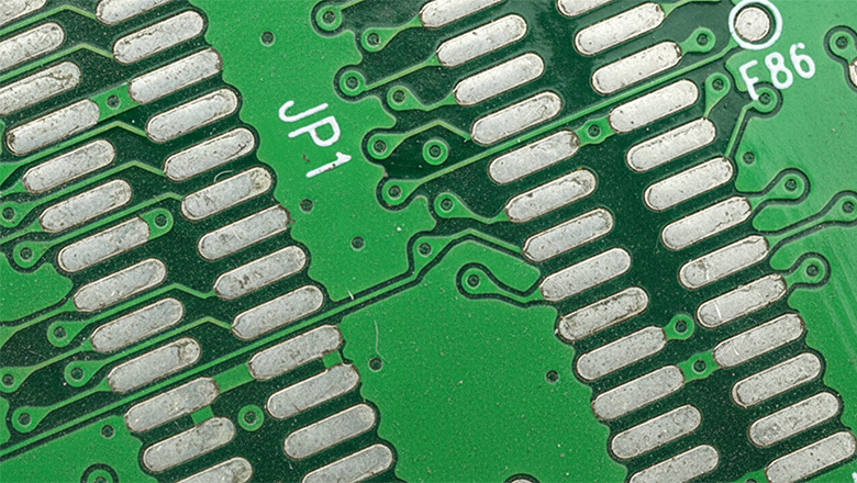
Through-hole pads are circular or oblong copper areas with a plated hole. Leads from traditional components are inserted into these holes and soldered, forming a reliable contact pad and strong mechanical anchor. The diameter of the pad here is crucial—too small and the component won’t fit, too large and the solder joint is weak.
Surface Mount Pads (SMD Pads)
These pads feature a rectangular or oval copper structure, located on the PCB surface without through-holes. Surface-mount devices are soldered directly onto the pad surface. The pad layout must precisely match the component package dimensions and appropriately sized pads help prevent soldering defects such as tombstoning and solder bridging.
NPTH Pads
NPTH refers to a pad that is Non-Plated Through-Hole, meaning the hole is not plated and is not intended for electrical connections, but for mechanical alignment (such as mounting holes or tool locations).
BGA, Test and Custom Pads
- BGA Pads:For Ball Grid Array components, pad arrangements are in dense matrices, with each tiny pad supporting a solder ball connection.
- Test Pads:Circular or square pads spaced for probe access in testing.
- Custom Pads:Used in custom PCBs, dome switches or high-power connections.
Pad Shapes and Arrangements: Matching Pads to Your Circuit Board Needs
The pad shapes in PCB design aren’t arbitrary—they’re engineered to support optimal solder flow, mechanical stability and electrical contact with the smallest real estate possible.
Common pad shapes and their recommended use:
| Pad Shape | Best For | PCB Technology Examples |
| Circular | Through-hole resistors, diodes, basic SMDs | Single-sided pcb, multi-layer pcb |
| Rectangular | SMD ICs, capacitors, connectors | High-density pcb, BGA mounting |
| Oval/Oblong | Connectors, power components | Power boards, custom pcb |
| Square | Test and fiducial pads, special land patterns | Keypad pcbs, alignment features |
| D-shape | Polarized connectors, USB, HDMI | Mixed-technology boards |
| Custom | Dome switches, RF connectors, special cases | Custom pcb designs |
A pad layout mirror is a technique where the pad arrangement on one side of the board matches the other, enabling double-sided assemblies and easier board stacking.
How to Specify the Proper Pad Size and Pad Arrangement
Determining the appropriate pad size is a skill that requires balance. An excessively small size will lead to poor soldering. An overly large size is prone to causing solder bridging and component misalignment. Achieving an optimal pad size design requires compliance with industry standards and the use of professional calculation tools.
Factors that determine the size of pads in PCB:
- Component Lead Style and Size – The pin or ball diameter, shape and type (THT, SMT, BGA) dictate the pad’s dimensions.
- Assembly Technique – Hand soldering allows slightly larger pads vs. machine assembly (where too large impacts component alignment).
- PCB Fabrication Tolerances – Real-world variances in etching, drilling, and plating impact the final pad dimension, so always allow for manufacturing tolerances when choosing your pad size.
- Soldering Process – Reflow, wave, and selective soldering each have ideal pad sizes for reliable, void-free joints.
- Pad Arrangement and Density – Higher density requires more precise pad layouts to prevent shorts and support correct solder mask design.
PCB Pad Stack, NPTH and Advanced Pad Details
What is a PCB Pad Stack?
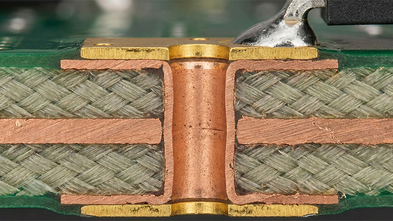
A pad stack defines the physical shapes, finishes and layers of a pad through all layers of the PCB. It includes:
- Top and/or bottom copper pad shape and size
- Drilled hole size (if any), through all layers
- Plating thickness (for PTH)
- Internal layer pads for multilayer boards
- Solder mask aperture — the opening in the solder mask that exposes the pad area
Why is Pad Stack Important?
Every contact pad must have a defined pad stack, especially in multilayer PCB, HDI PCB or when supporting complex components like BGAs. The design software tools let PCB designers define each layer’s pad geometry, so the PCB fabrication process can provide PCB features that match both design and assembly requirements.
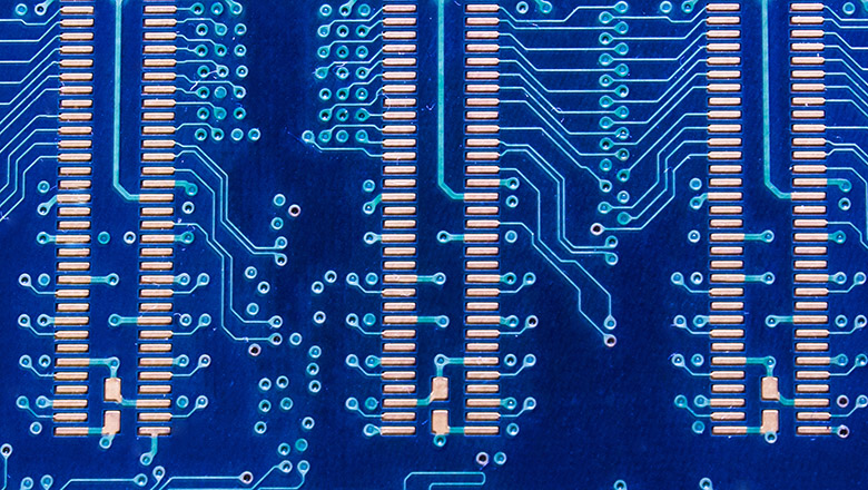
Pad Layout Mirrors: How Good PCB Layout Uses Optimized Pads

A robust pcb layout is all about alignment and symmetry. Good pad arrangements mean that:
- Parts are easy to place, inspect, and solder
- Solder joints form correctly during reflow, wave or hand soldering
- Test points and vias line up for efficient debugging
In complex assemblies, pad layout mirrors may be used—where the pad arrangement is symmetric on both sides of a double-sided pcb or in dual-row connectors where each row’s pad position “mirrors” the other.
In high-density circuit board design, pad layout is critical. The design must ensure consistent pad spacing. All pads should facilitate soldering, inspection and rework operations. It is essential that each pad remains operable on the PCB surface, and its layout complies with spacing regulations, solder mask requirements and routing principles.
Pad Design Mistakes and How to Avoid the Wrong Pad
Even experienced engineers can be tripped up by pad design mistakes! Here are the most frequent errors and how to avoid them in your PCB design and development:
Common Design Mistakes
- Pads That Are Too Small:Insufficient area leads to weak solder joints, unreliability or even floating/unattached components.
- Pads That Are Too Large:Risk of shorts, solder bridges and component misalignment.
- Wrong Pad Shape for Component Lead:Leads to incomplete soldering and poor electrical connections.
- Improper Pad Spacing:Pads placed too close together can cause accidental solder bridging, or may not pass electrical clearance checks.
- Ignoring PCB Fabrication Tolerances:Holes can wander during drilling, so always allow extra annular ring.
- Overlooking the Solder Mask Aperture:The mask opening should be a bit larger than the pad to ensure clean soldering and easy inspection.
- Not Using Standards or Calculators for PCB Pad Sizing:Guesswork is the enemy of yield and performance!
PCB Fabrication: How Pads Move from Design to the Surface of the PCB
The PCB fabrication process turns your pcb pad design into the physical copper pads visible on the surface of the pcb. Here’s how it works:
- Design:PCB designer specifies pads, vias and pad stacks in their PCB layout with design software tools. Pads in pcbs are reviewed and checked for accuracy.
- CAM Conversion:Your design is exported (often as Gerber files), which define where every pad must be for etching, drilling, plating and mask application.
- Fabrication:
- Pads are etched from copper, then plated (for PTH).
- The solder mask must have openings at the locations corresponding to the pads. For structures such as non-plated through-holes or other precision features requiring special attention. Additional inspection procedures must be implemented during the production process.
- Surface finish (ENIG, HASL, OSP, etc.) is added to ensure the pads accept solder reliably and resist corrosion.
- Assembly:Components are placed onto the PCB pads and soldered—by hand, wave or reflow process.
Establishing well-documented specifications and strictly implementing standards, combined with close communication mechanisms with the board manufacturer, enable the finished circuit board to accurately achieve the design objectives of each pad. This helps reduce the risk of high-cost losses that may arise after production is completed.
Conclusion: Provide PCB Designs with Careful Pad Choices
Pads may be the smallest features in a printed circuit board, but careful pad design brings benefits at every stage—from prototype assembly to full production. By following best practices, leveraging calculators for pcb pad, and working closely with partners in pcb fabrication and assembly, every PCB designer can ensure their circuits are robust, repairable and ready for the future.