Introduction
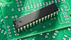
The electronics industry is undergoing rapid development, and the evolution of PCB design is advancing at an ever-increasing pace.A reliable and high-performance PCB cannot be achieved without one critical component: the solder mask.This polymer layer covers the top and bottom surfaces of the PCB, and functions to protect the internal critical copper traces, pads and circuits.
The selection and application of an appropriate solder mask are critical for both mass production and prototype development of innovative IoT devices.The solder mask in a PCB serves a dual function: it ensures stability during the assembly process and prevents abnormal solder dispersion to avoid unintended electrical connection between adjacent solder joints—the latter being the primary cause of circuit board defects.
This guide will cover multiple key dimensions: the specific application process of solder mask, the design principles for solder mask openings and solder mask bridge widths, the comparison of different solder mask materials and their pros and cons, as well as the critical points of Design for Manufacturing (DFM).These contents are intended to help developers avoid various potential defects, thereby maximizing the service life of PCBs.
Understanding the Solder Mask Layer in PCBs
What is a Solder Mask Layer?
The solder mask is a polymer coating applied during the PCB manufacturing process.It covers the top and bottom surfaces of the circuit board to form a protective layer, leaving only the solder pads to be soldered and some test points exposed.
- The mask is applied after copper etching and before silkscreen printing or assembly.
- The layer of solder mask ensures only designated, exposed pads can bond with molten solder during soldering.
Key Functions of the Solder Mask Layer:
- Prevents Solder Bridges:The solder mask covers the surface of copper traces.This physical isolation effectively prevents solder bridging between closely spaced traces or pads.For high-density surface mount technology (SMT) and high-density interconnect (HDI) designs, this protective mechanism is critical to the success of the overall design.
- Insulation and Environmental Protection:The solder mask provides multiple protective functions.This coating delivers essential electrical insulation and effectively prevents corrosion.It also safeguards against physical scratches during handling, environmental oxidation, dust contamination, and moisture erosion.This protective mechanism takes effect from the early stages of the circuit board’ s service life, effectively preventing various defects and avoiding board failure.
- Enables Precision in Assembly:It helps keep molten solder confined to intended pads, so it doesn’t spread where it could cause shorts or poor connections.
- Supports Solder Paste Application:Areas not covered with solder mask are specifically defined for paste mask, ensuring the right amount of solder paste is applied.
Why the Solder Mask is Critical in PCB Design
PCB solder mask plays a critical role in overall board performance, especially as circuits become denser and parts move closer together. The mask layer in a PCB is not just a cosmetic feature-it:
- Reduces defect rates in sensitive SMT and BGA layouts.
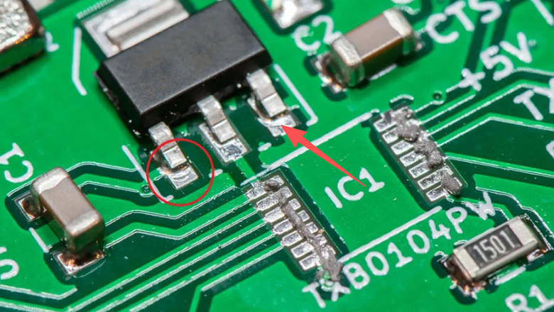
- The openings in the solder mask remain clearly defined, and the chosen color provides sufficient contrast. This design allows issues with soldering quality to be directly observed, while also facilitating the operation of Automated Optical Inspection (AOI) systems.
- The solder mask covers the various layers of the PCB, serving to resist physical stress and erosion from environmental factors.
- The solder mask possesses the ability to resist delamination. This characteristic allows it to maintain firm adhesion to the PCB substrate even after undergoing the thermal cycles of the soldering process. This stability forms the foundation for the long-term reliability of the circuit board.
Layers of the PCB and Where the Solder Mask Fits
A typical multilayer PCB’s cross-section:
| PCB Layer | Function |
| Silkscreen | Labels, reference designators (top & bottom) |
| Solder Mask | Protective layer that covers non-soldering areas |
| Copper | Traces, pads, and ground/power planes |
| Dielectric | Substrate (FR4, Polyimide etc.) |
| Copper | Internal routing, planes |
| Solder Mask | (If double-sided, on both top and bottom) |
The solder mask layer in PCBs is found just above the copper and under the silkscreen (legend text), protecting nearly all of the top and bottom layers except for exposed areas specified for soldering or testing.
Types of Solder Mask and Solder Mask Materials

Different Types of Solder Mask
Mask is applied using several methods depending on design requirements and manufacturing volume:
1. Epoxy Liquid Solder Mask
- Screen printed and thermally cured. This older mask material is cost-effective but less precise, best for low-density or prototype PCBs where mask apertures don’t need tight registration.
2. Liquid Photoimageable (LPI) Solder Mask
- Sprayed or curtain coated, imaged by UV light, and developed—ideal for modern PCBs, especially those with fine-pitch components or BGAs.
- Enables tight solder mask expansion, precision in minimum web width between mask apertures, and better adhesion to the PCB.
3. Dry Film Solder Mask
- Laminated using heat and pressure, patterned via photolithography, and developed. Dry film is common in flexible or rigid-flex boards, offering high control over thickness of the solder mask and superb bend resistance.
4. Peelable Solder Mask (Temporary Mask)
- Used only during assembly for process-specific needs (like protecting gold fingers). This mask is a temporary polymer layer that is physically peeled off before the board is put into final service.
Comparison of Types of Solder Mask
| Type | Application | Pros | Cons | Best Use |
| Epoxy Liquid | Screen Printing | Low cost, accessible | Coarse apertures, thick | Prototypes, hobby |
| LPI | Spray/UV Imaging | Fine features, precise | Universal SMT/HDI | Most PCBs |
| Dry Film | Roll Laminating | Bendable, uniform | Specialized, costlier | Flex/rigid-flex PCBs |
| Peelable | Manual/Semi-auto | Temp, easy removal | Not a permanent solder resist | Selective soldering |
Common Solder Mask Colors and Mask Materials
The most common solder mask color is “PCB green,” but blue, black, red, yellow, and white are all seen—each with different properties tied to pigment, mask materials, and UV absorption.
Why Green?
- Provides excellent contrast for AOI and visual inspection.
- Mature, reliable pigments and resins for best coverage and defect resistance.
Alternative Colors:
- White (optimal for LED PCBs), Black (stealth for consumer), Red/Blue for prototyping or branding.
- Note: The type of solder mask pigment used can influence the achievable minimum solder dam width. Consequently, adjustments to the solder mask expansion and related design rules are necessary during the design phase.
Choosing the Right Solder Mask Material
- Match solder mask type to your PCB design requirements. For most SMT and HDI PCBs, an LPI solder mask is optimal due to its precision, reliable adhesion to the PCB, and superior capability to define fine apertures and minimum web width. For flexible circuits, select a dry film solder mask that remains robust through bending cycles.When designing the solder mask layer, consider these additional factors regarding mask materials:
- Environmental resistance: Some mask materials stand up better to solvents, soldering heat, or outdoor exposure.
- Mask expansion limits: Every mask type and color comes with recommended expansion and minimum spacing rules—check your fab’s DFM guidelines for solder mask design before signoff.
- Manufacturing process compatibility: Not every fab supports all solder mask types or colors equally. Confirm availability and process controls before finalizing design files.
The Role of Solder Mask in PCB Assembly and Manufacturing
The solder mask layer in PCBs plays a critical role throughout the manufacturing process and during PCB assembly:
Preventing Solder Bridges and Controlling Molten Solder
The solder mask performs the function of preventing the formation of solder bridges. A solder bridge is a soldering defect caused by the spreading of molten solder between adjacent copper conductors during reflow or wave soldering. The solder mask defines precise aperture areas to delineate where solder can wet, while acting as a permanent barrier covering other conductor surfaces. This mechanism ensures that solder contacts only the intended pads, fundamentally eliminating the occurrence of solder bridges.
Solder Mask Layer as a Protective Layer
After the copper pattern fabrication is completed, a solder mask coating is applied to the surface of the PCB.This coating physically isolates most of the copper surface from solder, air and moisture; this isolation ensures circuit integrity and prevents the copper layer from corrosion, abrasion and environmental degradation.
Interface With Paste Mask
The paste mask is another essential part of PCB manufacturing. Unlike solder mask (a permanent layer), the paste mask is the pattern used to apply solder paste to component pads before reflow. During paste stencil creation, only the mask apertures (openings) where solder paste is to be applied are defined—often lining up with the open regions in the solder mask layer.
Remember:
- Paste mask is temporary, created for each assembly run.
- Solder resist (mask) is a permanent polymer layer; paste mask is used only during assembly.
Guidelines for Solder Mask Design in Modern Manufacturing
Every modern fab uses robust DFM guidelines for solder mask to ensure yield and reliability:
- Minimum solder mask expansion to ensure mask never creeps onto pads.
- Defined mask web width to prevent slivers and peeling.
- Clearly specified mask materials for environmental requirements.
- Mask thickness and adhesion tests as part of the QA process.
Step-by-Step: Solder Mask Application Process in PCB Manufacturing
Layer by Layer: Top and Bottom Sides
In the manufacturing of a typical double-sided circuit board, a solder mask is applied to both the top and bottom surfaces—excluding the openings reserved for pads, vias, and test points. This dual-side coverage structure forms a comprehensive protective mechanism throughout the assembly and operation cycle, thereby ensuring product reliability.
Solder Mask Application Steps
- Board Cleaning:Panels are meticulously cleaned. Any contamination will prevent proper adhesion.
- Mask Coating:Epoxy, LPI, or dry film mask is applied depending on the design and fab setup.
- LPI mask is sprayed or curtain coated as a liquid.
- Dry film mask is laminated on via rollers and heat.
- Soft Bake (For LPI):A gentle bake solidifies the mask, making it photosensitive.
- Photolithography Imaging:A photo-tool (or direct laser) exposes defined mask openings (apertures) for pads, vias, etc. UV cures exposed areas of the mask.
- Developing:Unexposed mask is washed away, leaving precise apertures.
- Final Bake:The mask is fully cured for maximum chemical resistance and structural strength.
- Inspection & Thickness Check:AOI systems or manual checking verify registration, absence of blisters, and adherence to thickness and coverage requirements.
Solder Mask on Top and Bottom Sides
The uniformity of solder mask thickness on the top and bottom layers directly impacts the feasibility of the design. Controlling this parameter becomes particularly critical when the circuit board design involves microvias, cavity structures, BGA packaging, or flexible boards and castellated holes.
Solder Mask vs. Paste Mask
- Solder mask: permanent protective polymer layer, defines where not to solder.
- Paste mask: temporary pattern for applying solder paste, defines exactly where solder paste is applied for assembly.
- Both must work together seamlessly for a properly assembled PCB.
Designing the Solder Mask Layer: Rules, Expansion, and Thickness
Applying Design Rules and Mask Expansion
Every PCB EDA tool provides fields for solder mask expansion (the difference between pad size and mask aperture), minimum web width (distance between adjacent openings), and the use of via tenting/covering.
Design rule highlights:
- Standard solder mask expansion: +0.05 mm to +0.10 mm per pad edge.
- Minimum web width: ≥0.10 mm (0.125 mm for some mask materials/colors).
- Expansion and web width must always follow fabricator’s guidelines for the selected solder mask material.
Minimum Solder Mask Features & Common Defects
- Too-narrow mask webs or insufficient mask expansion can lead to mask slivers, which peel from the board after soldering.
- Mask overlapping pads (negative expansion) causes solder starve and poor assembly yield.
- Too much expansion exposes more copper, risking corrosion and solder wicking.
Thickness of the Solder Mask Layer
- Standard: 18–38 microns; critical for insulation, environmental protection, and mechanical resistance.
- Consistency of thickness is vital—thinner mask means less protection, thick mask may flood small openings.
- You should always specify thickness if your board is intended for harsh environments or involves fine-pitch SMT.
DFM Guidelines for Solder Mask: Top 4 Best Practices
1. Maintain Proper Solder Mask Clearance & Expansion
- Set mask apertures to be 0.05–0.10 mm larger than pad on all sides.
- Ensure web width remains ≥0.10 mm green, 0.125 mm other colors.
2. Use Appropriate Via Tenting or Covering
- Tenting: mask covers via. Necessary to prevent solder wicking, especially under BGAs or HDI fanout.
- If via must remain open for testing, specify in your fabrication notes.
3. Optimize Silkscreen and Mask Interaction
- Avoid silkscreen legend over exposed pads or critical mask features.
- Minimum separation typically 0.15 mm.
4. Choose Right Mask Thickness for Application
- Thicker mask for automotive, power, and industrial; fine, uniform mask for RF, HDI, and flex boards.
Advanced Considerations: Adhesion, Testing, and PCB Reliability

Adhesion to the PCB and the Solder Resist Application Process
Adhesion of the solder mask to the surface of the PCB substrate is the fundamental prerequisite for it to provide long-term protection and electrical isolation.Surface residues must be strictly controlled during the solder mask application process.Ensuring substrate cleanliness serves a dual purpose: it guarantees firm adhesion of the polymer layer covering the copper surface, and prevents the solder mask material from peeling off during soldering or when exposed to solvents.This requirement applies throughout the entire modern PCB manufacturing and assembly process.
- Pre-bake steps and chemical cleaning enhance long-term adhesion, reducing mask lifting and field defects.
- Ensuring that the mask is properly cured eliminates risk of delamination during the thermal cycles of reflow or wave soldering, even as molten solder flows and the mask layer is challenged by temperature changes.
Solder Mask Expansion and Mask Web Width – Practical Reliability
For each pad, via, and exposed copper area, setting the right solder mask expansion is vital. This “halo” of extra mask opening (the solder mask expansion) compensates for registration tolerances in the manufacturing process, ensuring reliable mask openings. It’s also closely tied to defect prevention:
- Too little solder mask expansion can lead to the mask creeping onto pads and causing solder defects.
- Too much leaves more copper exposed, increasing the risk of oxidation, especially in parts of the PCB subject to environmental stress.
Minimum solder mask web width—the narrowest strip of solder mask between apertures—is equally important. If the web is too thin, slivers can break off, causing random defects across batches. Following the fab’s recommended web size (0.10 mm for green, 0.125 mm for other mask colors) is a proven best practice.
Solder Mask QA, Visual Inspection, and Electrical Testing
After manufacturing, each board’s mask layer is visually inspected and, in critical markets, tested for:
- Registration and coverage (Do all pads, vias, and mask apertures align with the design requirements?)
- Thickness of the solder mask (Spot-checked with profilometers or by cross-section.)
- Adhesion and tape test (To ensure the mask is not easily removed by mechanical or thermal shock.)
- AOI and electrical shorts testing (Finding solder from bridging or mask slivers hidden under BGA.)
Advanced manufacturers also run field-specific tests (like humidity, salt spray, or solderability testing) for automotive, aerospace, and medical markets—environments where the solder mask plays a critical role in field reliability.
Frequently Asked Questions About Solder Mask in PCB Design
Q1: What’s the difference between solder mask and paste mask?
A: The solder mask layer is a permanent, insulating, protective layer applied to a PCB to keep molten solder from spreading and prevent solder bridges. Paste mask refers to the temporary pattern—created with a stencil—used to apply solder paste only where needed during assembly.
Q2: How does the mask layer interact with solder paste?
A: Solder paste is applied to exposed copper pads (open mask apertures) as defined by the paste mask. The tight control of solder mask ensures that only pads get solder paste—supporting precise, defect-free assembly.
Q3: Does mask color matter for PCB performance?
A: While the most common solder mask color is green, color mostly affects visual inspection—green offers the best contrast for AOI. Each color formulation has slightly different process tolerances and minimum web widths; always check with your fab.
Q4: What is the defect most often seen with improper solder mask application?
A: The most common solder mask defect is solder bridging from insufficient web width or improper mask expansion, causing shorts between adjacent pads or traces. Mask slivers and mask overlap are also classic issues that proper DFM and mask design rules prevent.
Q5: Can solder mask be applied only to the top or bottom?
A: While possible, good PCB design covers both the top and bottom layers of the PCB with solder mask, maximizing protection and reliability. Some single-layer or special purpose boards may mask only one side if needed.
Q6: Why is the solder mask also called solder resist?
A: Because it resists the flow and spread of molten solder during assembly, keeping solder where it is needed—which is why it’s sometimes still called a solder resist layer.
Q7: What are guidelines for solder mask design expansion values?
A: Use your fab’s proven defaults—typically 0.05–0.10 mm solder mask expansion on all sides, minimum solder mask web width of 0.10 mm (green) or 0.125 mm (non-green), and always tune for manufacturing process variation.
Conclusion: Mastering Solder Mask in PCB Manufacturing
The solder mask layer in PCBs is your board’s silent guardian, protecting copper, enforcing assembly precision, and delivering long-term field reliability. By respecting process guidelines, specifying the correct mask layers and mask materials, and always applying rigorous DFM guidelines for solder mask, you’ll ensure every board is robust against defect, easy to assemble, and safe from random field failures.
For PCB designers, manufacturing engineers, and procurement professionals, the message is clear: invest in correct solder mask specification and integration from day one. Communicate clearly with your fab on mask type, thickness, expansion, and inspection. Stay current with IPC and industry standards. And always treat the solder mask as not just a coating, but a mission-critical layer of your next great electronic innovation.