Introduction to PCBA in Modern Electronics Manufacturing

The advancement of modern electronics manufacturing relies on two core processes: one is the fabrication of printed circuit boards, and the other is the assembly of these boards into fully functional electronic devices. PCB Assembly, commonly referred to as assembly, is the process that transforms bare boards consisting solely of substrates and copper traces into stable and operational end products.
PCB vs. PCBA: Understanding the Difference in the PCBA Manufacturing Process
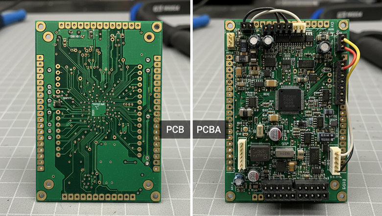
A bare PCB is a physical platform—a substrate layered with copper traces, solder mask, and silkscreen. It offers the foundation for electronic circuit creation. However, these raw boards cannot function until they pass through the PCBA manufacturing process.
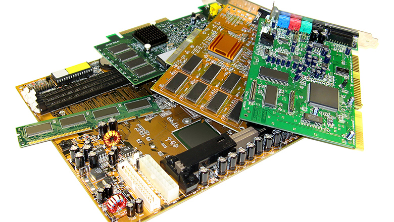
PCBA,or PCB Assembly.It refers to the process of assembling all electronic components such as capacitors, resistors, integrated circuits, and connectors—onto a printed circuit board using techniques like surface mount technology (SMT) or through-hole technology (THT). The resulting complete unit is called a PCB assembly or assembled PCB. This process marks the critical transition of a circuit board from a design schematic into a fully functional electronic product.
Quick Comparison Table: PCB vs. PCBA
| Criteria | PCB (Printed Circuit Board) | PCBA (Printed Circuit Board Assembly) |
| Function | Physical structure, connections only | Contains all component and circuit functionality |
| Manufacturing Process | Etching, laminating, applying solder mask/silkscreen | Assembly, soldering, testing of electronic components |
| End-Use | Not functional alone | Ready for integration into electronic products |
PCB Design Basics: Paving the Way for Reliable PCB Assembly
High-quality assembly starts with a manufacturable and practical PCB design. Here are some key points covered in any guide to PCB assembly:
Key Concepts:
- PCB design basics include planning the placement of copper traces, solder mask, and component pads.
- Layout design shall handle surface mount components and through-hole components simultaneously. The diameter of each drill hole must accurately complywith the specifications. The size and positioning of each pad must also be completely accurate.
- Modern printed circuit board assemblies are divided into three primary categories. These are rigid printed circuit board assemblies, flexible printed circuit board assemblies and rigid-flex combination printed circuit board assemblies. The manufacturing of different assembly types requires the selection of specific foundational materials. These assemblies also employ distinct multi-layer lamination structural designs.
Design for Manufacturing (DFM): Design for Manufacturing principles guide that circuit board designs must meet the requirements for high-efficiency production and stable batch replication. The design phase requires panelization layout to enable multi-board joint manufacturing. Silk-screen markings must maintain clear isolation from solder pad areas. Each functional layer should reserve sufficient operational clearance to support the complete assembly process.
Overview of the PCBA Process
The PCBA process is often described as a journey—the process steps systematically transform a schematic plan into a real, assembled electronic circuit. This pcb assembly process includes numerous stages, each designed for maximized yield and process control.
Essential Steps in the PCBA Process:
- Component procurement
- Incoming quality control and storage
- Preparation and cleaning of bare PCBs
- Stencil design and solder paste printing
- Component placement (pick and place)
- Soldering (reflow or wave soldering)
- Inspection and quality control (AOI, X-ray)
- Functional electronic testing (ICT, FCT)
- Final cleaning and packaging
Printed circuit board assembly technology exhibits broad applicability. Its application scope encompasses various printed circuit board structures, ranging from basic single-layer printed circuit boards to advanced multilayer printed circuit board assemblies.
Preparation Before the PCB Assembly Process: Best PCBA Manufacturing Practices
Thorough preparation sets every quality assembly apart.
- Bill of Materials (BOM):List every part for sourcing and quality validation.
- Incoming Inspection:Every batch of electronic components and bare circuit boards must undergo IQC to catch discrepancies or counterfeits.
- PCB Cleaning:Prior to any solder being applied to the PCB, ultra-sonic cleaning or specialized solvents may be used to remove potential contaminants from the PCB surface for reliable soldering.
- Stencil Preparation:Stencil design is critical. The stencil controls how much solder paste is deposited onto the PCB pads, directly impacting solder joint quality.
Step-by-Step PCBA: Detailed Guide to PCB Assembly
Let’s walk through every important step of the printed circuit board assembly process.
1. Solder Paste Printing
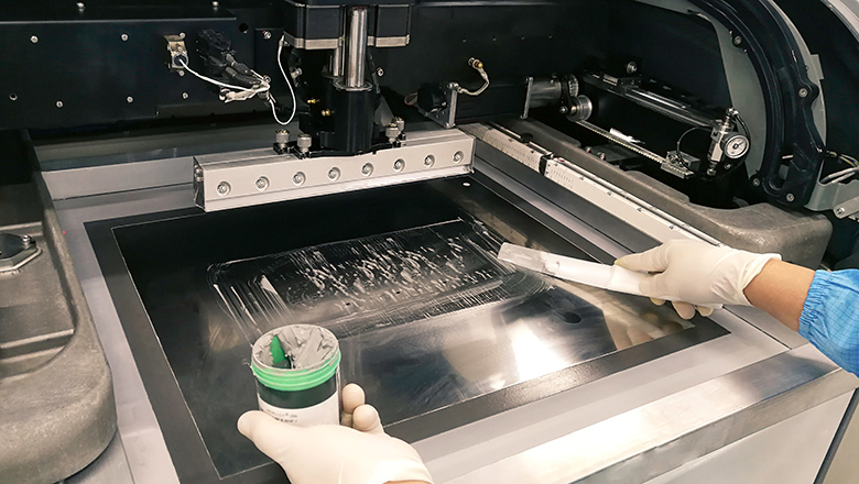
The first major step of PCB assembly is applying solder paste to the PCB pads using a metal stencil. The process involves:
- Placing the stencil above the bare PCB.
- Spreading solder paste over the stencil, which passes through the stencil openings and deposits precisely onto the PCB pads.
- Solder paste management is crucial for assembly quality: always ensure paste is fresh and evenly applied.
2. Component Placement (Pick and Place Process)

Using an automated pick and place machine, components are placed rapidly and accurately:
- The pick-and-place machine first scans and identifies the position of each pad on the circuit board. The equipment then automatically mounts electronic components onto designated areas of the printed circuit board. During the mounting process, precise alignment of component orientation is simultaneously achieved. This series of operations collectively enables high-precision automated assembly of components.
- In the prototype development or repair scenarios of electronic products, production personnel may adopt manual methods for component placement. For large-scale mass production, automated PCB assembly demonstrates significant advantages. This approach enables exceptionally high production speed. It also ensures consistent product quality. Its placement accuracy far exceeds that of manual operations.
3. Pre-Reflow Inspection

Before soldering, vision systems or AOI machines verify that:
- The right amount of solder paste was applied to the pcb pads.
- Each electronic component is correctly aligned and fully seated.
4. Soldering: Reflow and Wave Soldering

The reflow process is standard for most surface mount assemblies:
- The PCB assemblies pass through a reflow oven with temperature-controlled zones.
- The soldering process involves passing the board through preheat, soak, reflow (where solder melts and bonds components), and cooling stages.
- The assembly of through-hole components requires the use of wave soldering technology for welding. This process allows the circuit board to pass smoothly through a wave of molten solder formed during operation. The solder fully fills each metallized hole on the printed circuit board. The component leads form a secure and reliable connection with the hole walls through the solder.
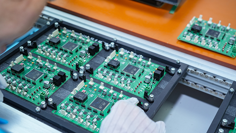
5. Inspecting the PCB (AOI, X-ray, and Manual)

In the printed circuit board assembly process, the inspection stage commences immediately after completion of the core soldering operation. This stage serves as the critical control point for ensuring assembly quality.
- Automated Optical Inspection (AOI):Advanced AOI systems scan both the top and bottom of the board, comparing each assembled board to a reference model. This step detects missing, skewed, or misoriented components, solder bridges, and insufficient solder paste. Automated PCB assembly lines integrate AOI at multiple process steps—after pick and place, and post-reflow—to catch all potential errors.
- X-ray Inspection:For modern high-density assemblies, such as BGAs or QFNs, X-ray inspection is used to “see through” the circuit boards, revealing hidden solder joint defects (voids, cold joints) that could affect a functional electronic circuit.
- Manual Inspection:Skilled technicians also visually inspect the board for any anomalies that machines may miss, verifying assembly against PCB design files and BOM.
6. Through-Hole (THT) and Mixed Assembly Processes
Not all electronic components are suitable for SMT assembly. Through-hole components—such as connectors, large capacitors, transformers, and power devices—require special treatment:
- Components are inserted into pre-drilled holes in the PCB.
- The bottom of the board undergoes soldering by being passed across a wave of molten solder (wave soldering process).
- THT assembly is often combined with SMT in mixed assembly; this approach leverages the strengths of both technologies for complex circuits.
7. Functional Testing and Final Inspection

After completing all physical assembly processes, each printed circuit board assembly must proceed to the testing stage. The testing phase is required to verify the craftsmanship quality of the assembly. It also needs to examine the performance of the entire electronic circuit.
- In-Circuit Testing (ICT):Probes contact test points or pads on the PCB to measure resistance, capacitance, shorts, and opens.
- Functional Test (FCT):Simulates real-world use: all interfaces, sensors, and outputs are checked under operational conditions, confirming the PCBA performs as a fully functional circuit.
- Burn-in Test:For mission-critical boards, the assembled PCB is subjected to prolonged operation cycles, power cycling, and varied temperatures to weed out premature failures.
8. Cleaning, Packaging, and Logistics

Assembled printed circuit boards must undergo a cleaning process after passing all inspection steps. The purpose of cleaning is to remove residual solder flux and various contaminants. These substances may compromise the long-term reliability of the product. Modern cleaning technologies offer multiple technical solutions, primarily including aqueous cleaning methods, semi-aqueous cleaning methods, and no-clean process solutions.
Boards are packaged—often in anti-static bags or trays—for protection during storage and shipping. Each step of PCB assembly involves process control to ensure no static or moisture affects the electronic assembly before final integration.
Assembly Methods: SMT Assembly, THT Assembly, and Mixed Assembly
There are multiple pathways for the assembly of printed circuit boards, each suited to different PCBA manufacturing needs.
Surface Mount Technology (SMT Assembly)
- Enables mounting of components directly onto one or both sides of the board.
- Achieves the smallest electronic circuit footprint and the highest assembly speed.
- All process steps, from solder paste application to automated pick and place, are highly automated for consistency and cost-efficiency.
Through-Hole Technology (THT Assembly)
- Components are placed through holes in the PCB and soldered from the bottom.
- Ideal for connectors, inductors, and components needing mechanical strength.
- Soldering involves passing the board over a wave; this process step offers strong attachment but uses more PCB real estate.
Mixed Technology Assembly
- Also called hybrid assembly, it combines SMT and THT on a single PCB.
- Typical in advanced circuit board designs and in product assembly requiring both dense logic and rugged I/O.
PCBAQuality Assurance and Inspection

Assembly quality in the PCBA process is guarded by systematic inspections, standards compliance, and process audits.
- Leading PCBA manufacturers are certified to ISO9001, IPC-A-610, and often RoHS.
- Process control at every stage is vital: from verifying solder paste on the pcb pads, to validating all circuit boards against the PCB design files and assembly drawings.
- Routine audits of the assembly process catch deviations early, while statistical process control (SPC) monitors metrics like defect rates, solder joint quality, and machine calibration.
Choosing a PCBA Manufacturer: Delivering Reliable PCB Assembly and PCBA Services
Selecting the right printed circuit board assembly partner is essential for reliable product assembly.
Key selection criteria include:
- Full spectrum PCB and PCBA manufacturing capabilities (prototype, pilot, production).
- Transparent process steps and robust process control.
- Proven track record in advanced circuit board assembly methods (SMT and THT).
- Integrated in-house testing, inspection, and NPI engineering support.
- Certifiable regulatory compliance: ISO, IPC, RoHS, and more.
PCBA Manufacturing Cost Factors
Cost in PCBA manufacturing is a function of:
- PCB complexity (layers, materials, finishes)
- Component count and package types (BGAs, SMDs, through-hole components)
- Volume of assemblies (automated PCB assembly scales well)
- Testing and inspection requirements
- Speed of delivery (expedited assembly commands premium)
Trends, Innovations, and the Future of PCB Assembly
Automated PCB assembly continues to evolve:
- AI-augmented process steps, real-time analytics, and predictive machine learning are emerging for defect detection and process control.
- Green manufacturing processes emphasize halogen-free materials, lead-free solders, and low-VOC cleaning.
- Enhanced process visualization tools (digital twins, AR for assembly) help verify assembly steps and train operators.
- Rapid prototyping platforms now offer turnkey PCB assembly services, helping startups quickly iterate from PCB design to product assembly.
FAQs About PCB Assembly
Q: What files do I need for a turnkey PCBA services quote?
A: You’ll need Gerber files, pick and place data, PCB design files, silkscreen info, BOM, and test instructions.
Q: How do you ensure surface mount components are seated correctly?
A: After the pick and place process, AOI and X-ray inspect each PCB assembly for correct component placement onto the printed circuit board.
Q: What’s the difference between PCB and PCBA?
A: A PCB is just the bare circuit board; a PCBA is a complete, functional electronic assembly with all components and soldering completed.
Conclusion: Best Practices in PCBA and Assembly
The printed circuit board assembly process bridges innovation and practical product realization in modern electronics manufacturing. Whether you are building a proof-of-concept prototype or scaling to mass production, understanding every assembly step—from pcb design basics and the application of solder paste on the pcb pads, to advanced inspection and functional testing—is vital for successful, reliable assembly.
A robust pcba manufacturing process ensures that every functional electronic circuit meets quality standards, regulatory requirements, and your application’s unique technical demands. Choose partners who specialize in pcb and pcba manufacturing, offer transparent process control, employ both smt and tht assembly methods, and can support product assembly with stringent inspection and testing protocols.