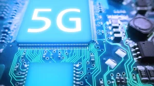
Introduction to Printed Circuit Boards

At LHD TECH, we recognize that the modern world is built on a foundation of electronic device. If you’ve ever used a smartphone, a computer, or any advanced device, you’ve directly experienced the innovation that LHD TECH enables through advanced Printed Circuit Board (PCB) technology.
For us, mastering printed circuit technology represents more than just manufacturing; it is the critical leap that makes true miniaturization, unwavering reliability, and efficient mass production possible. It is at the core of how we help bring visionary electronic concepts to life.
A PCB, as engineered by LHD TECH, serves a dual purpose: it is both the robust physical platform and the precise electronic roadmap for any device. We create connections between components through exacting circuit patterns, meticulously etched onto high-performance substrates—typically fiberglass or composite epoxy—ensuring optimal signal integrity and durability.
The PCBS made by our company can be said to be the “infrastructure” of modern electronic products. From the smart home devices and learning equipment at your fingertips to life-saving medical instruments and space systems in space – in almost all key devices in various fields, our circuit boards are supporting them behind the scenes. It can be said that every board we make is driving the progress of an industry.
What Is a Printed Circuit Board and Why Is It Needed?

A Printed Circuit Board (PCB) is a flat, skinny board—often green—used to build electronic circuits. It serves two main functions:
We define a Printed Circuit Board (PCB) as the fundamental engineered platform for modern electronics. More than just a flat, often green board, it is the precision canvas upon which we build reliable electronic circuits.
We engineer every PCB to perform two critical functions:
- Mechanical Support: Our boards provide a solid, stable foundation to securely mount and hold electronic components—from sophisticated microchips to essential resistors and capacitors.
- Electrical Interconnection: We replace bulky, error-prone wiring with a precise network of microscopic copper traces. This LHD TECH-designed circuitry ensures optimal signal flow and reliable circuit layoutand connections between components through a network of thin copper traces.
The architecture of an PCB is one of layered precision. We construct boards from one or more layers, each layer of a PCB includes a layer of copper for conducting electricity, expertly separated and supported by insulating substrate materials. The components are soldered to the board, creating both a physical anchor and a flawless electrical bond.
By mastering PCB technology, Our manufacturing process enables the design and manufacture of complex circuits that are vastly more reliable, consistent, and manufacturable than outdated point-to-point wiring. From a simple circuit to a multilayer supercomputer motherboard, we ensure the PCB remains the universal standard for translating visionary circuit designs into robust, high-performance physical reality.
Key Elements and Structure of a PCB
Here’s what a PCB consists of:
| Element | Description |
| Copper Layers | Thin sheets of copper printed onto the substrate; create the circuit pattern inside the board. |
| Substrate | The foundation or base (FR4, polyimide, or metal core); gives the board its rigidity. |
| Solder Mask | Thin protective layer covering copper except at pads; prevents shorts and corrosion. |
| Silkscreen | White (or other color) labeling that helps identify components on the board and orientation. |
| Pads | Metal areas where components are soldered or placed for conductivity and strength. |
| Vias | Tiny holes on the PCB, used to build electrical connections within the board or across layers. |
| Traces | Copper “wires” or lines (sometimes called circuit layout) that connect components in the circuit board. |
| Bare Board | An empty circuit board (no components), just the substrate, copper, mask, and silkscreen. |
Types of PCBs
Depending on the application and function, there are many different types of PCB:
| Type of PCB | Description and Applications |
| Rigid PCB | The most common PCB; rigid board offers robust support and is found in computers, TVs, and appliances. |
| Flexible Circuit | Built on polyimide substrate, bends or twists to fit tight/odd-shaped spaces—vital in cameras and wearables. |
| Rigid-Flex PCB | Hybrid of rigid and flex used for compact, rugged electronics (military, aerospace, smartphones). |
| Multi-layer PCB | 3+ copper layers (some with 20+!)—essential in computers, network gear, and telecom base stations. |
| Single/Double-sided | Simple circuits on one or both sides; found in entry-level consumer electronics. |
| Metal-Core PCB | Has an aluminum or copper core for maximum heat dissipation. Used in high-power LED PCBs, automotive lighting. |
| LED PCB | Specially designed for efficient LED mounting, cooling, and power delivery. |
PCB Design Process: From Idea to Board

Our approach to designing and manufacturing a printed circuit board follows a refined, professional workflow that ensures precision, reliability, and performance from concept to completion.
1. Schematic & Concept
Start with an intro to PCB desig,Our engineers define the circuit design in a detailed schematic, specifying all electronic components and their logical connections. We utilize industry-leading computer-aided design (CAD) tools such as Altium Designer and KiCAD to capture the circuit’s intent accurately from the very start.
2. PCB Layout
In this critical phase, we translate the schematic into a physical blueprint. Using advanced PCB design software, our team meticulously defines the board shape, optimizes component locations, and routes the intricate network of copper traces that form the connections between components. We strictly apply our comprehensive design rules—governing trace width, spacing, and via specifications—tailored to both manufacturing excellence and the demands of the functional circuit.
3. Simulation & Review
Prior to fabrication, every design undergoes rigorous validation. We perform simulations to check signal integrity, power distribution, and EMI performance, ensuring the design of the PCB meets all operational, safety, and reliability standards. A final, thorough review includes automated and peer-driven design rule checks to guarantee the PCB layout is optimized for manufacturability.
4. Generate Manufacturing Data
We prepare the complete data package for production. This includes generating precise Gerber files—the universal standard for communicating board specifications such as copper layers, solder mask, silkscreen, and drill patterns. LHD TECH supplements this with a detailed Bill of Materials (BoM) and clear assembly drawings to ensure flawless component placement.
5. Choose Board Designs & Materials
The physical foundation of the PCB is selected with the application in mind. Our experts guide the selection of the substrate—whether standard FR4—most common PCB, flexible polyimide, or robust metal core—along with copper weight, surface finish, and the complete board stackup. This material science is integral to achieving the desired performance, durability, and form factor.
PCB Manufacturing Process: How a PCB is Made
Now that your pcb design is finalized, here’s how a board is formed:
Step-by-Step Manufacturing Process
| Step | Description |
| 1. Blank PCB Creation | Laminate layer of copper onto substrate (FR4, metal core)—forms a blank sheet ready for fabrication. |
| 2. Photoresist Application | Apply light-sensitive film to the surface of the PCB. |
| 3. UV Exposure | The board is exposed to UV light through film/photoplot to outline circuit patterns. |
| 4. Etching | Removes unprotected copper, leaving only circuit layout (the traces, pads). |
| 5. Drilling Holes | All via and through-holes are drilled, often by CNC for precision. |
| 6. Plating | Holes are plated with copper, creating connections inside the board between layers. |
| 7. Solder Mask | Applied to the board for insulation and protection, exposing only pads and holes for soldering components. |
| 8. Silkscreen | Applies labels, part numbers, and markings so designers and assemblers can easily identify components on the board. |
| 9. Surface Finishes | Gold, silver, or other finishes are applied to exposed pads to improve solderability and long-term performance. |
| 10. Board Routing | The board is cut and shaped according to the design data, producing the final board shape. |
| 11. Final Inspection | Advanced inspection processes like Automated Optical Inspection (AOI), X-ray, and electrical tests check every blank PCB before assembly. |
In the view of LHD TECH, producing a PCB is far more than just making a bare board. This is the manufacturing process of meticulously transforming the design in your mind into a physical object. From the preparation of printed circuit board design to the conclusion of the final test, we strictly control every step: guiding production with precise engineering data, repeatedly checking with strict quality standards, and then selecting the most suitable plates and processes based on your specific needs.
It is precisely this close cooperation throughout the entire chain from design to manufacturing that enables every circuit board produced by LHD TECH to firmly exceed the industry’s strict requirements for reliability and manufacturability, and fully meet the needs of today’s high-end electronic products.
Applications: How PCBs Are Used in Modern Electronics

PCBs are used in virtually every sector by transforming sophisticated board layouts into tangible, real-world innovation. Our expertise lies in tailoring specific circuit board designs to meet the unique and demanding needs of each industry. Here are key examples of how we enable technological advancement:
Consumer Electronics
- Smartphones and Tablets:We enable the sleek, powerful devices of today by designing and manufacturing high-density multilayer PCBs and advanced rigid-flex boards. This allows us to pack immense processing power and global connectivity into incredibly thin and lightweight form factors.
- Wearables and Fitness Trackers:For devices that live on the body, LHD TECH utilizes durable flexible circuits that conform naturally to the wearer. We apply stringent design rules to ensure these boards withstand constant movement while maintaining ultimate reliability and comfort.
- Advanced Displays and Lighting: In applications from high-definition TVs to architectural lighting, our specialized LED PCB solutions, particularly metal-core PCBs(MCPCBs), provide the critical thermal management required for performance, efficiency, and longevity.
Automotive and Transportation
At LHD TECH, we engineer resilience for the road. For critical systems like engine management and infotainment, we deploy robust rigid and rigid-flex PCBs designed to endure constant vibration, extreme temperature fluctuations, and long-term operational wear. In enabling Advanced Driver Assistance Systems (ADAS), the core technology of LHD TECH – high-density Connected (HDI) PCB – plays a key role. This type of board can deploy high-speed signal channels in an extremely small space, precisely meeting the processing requirements of massive data from sensors, radars and cameras.
Aerospace & Defense
For those fields where errors are absolutely not allowed, such as avionics, navigation and communication systems, we offer top-notch reliable solutions. We use high-performance substrates such as polyimide to manufacture advanced multi-layer circuit boards. These boards were designed from the very beginning to target the harshest environments: repeated extreme high and low temperatures, continuous intense vibrations, and strong electromagnetic interference – they all have to withstand them steadily without any compromise on performance.
Industrial and Energy Sectors
We build the backbone of industry and infrastructure. LHD TECH supplies durable PCBs for power controllers, industrial robots, and grid communication devices. Our solutions often incorporate thick-copper, metal-core, and heavy-duty rigid boards, engineered specifically for superior current handling, efficient thermal dissipation, and unmatched physical durability in harsh environments.
Medical Devices
Precision and trust are paramount in healthcare. LHD TECH supports life-saving innovation by providing advanced circuit boards for devices like diabetes monitors and imaging equipment: We specialize in flexible and high-layer-count multilayer PCBs that meet the dual imperatives of flawless reliability and strict biocompatibility standards, ensuring patient safety and device efficacy.
PCB Design Rules, Tools, and Tips
PCB Design Software and Tools
We have always believed that professional PCB design tool is the key bridge to turning a good idea into a circuit board that can be actually produced. Our engineering team is proficient in various mainstream tools in the industry, such as Altium Designer, Cadence Allegro/OrCAD, Mentor PADS, etc. They are all very skilled at them.
From drawing the schematic diagram to repeatedly checking each circuit and the real operation of the analog circuit – throughout the entire development process, these software is used to our capable assistants. Finally, they can also help us generate a complete and error-free production document package, clearly arranging everything from Gerber diagrams, bill of materials to drilling files, ensuring that every design handed over to the factory is exactly as you imagined.
Design Rules Every PCB Designer Should Know
| Design Rule/Constraint | Purpose |
| Minimum Trace Width | Ensures each trace carries intended current |
| Copper-to-Copper Clearance | Prevents short circuits; key in HDI boards |
| Hole/Pad Sizing | Matches component leads and manufacturing limits |
| Solder Mask Clearance | Exposes just enough pad for soldering, shields rest |
| Board Edge-to-Copper Distance | Prevents arcing/shorting at board outline |
Common PCB Layout Best Practices
We implement foundational layout principles to ensure optimal performance and serviceability. We strategically group related components on the board to minimize trace length, reduce noise, and enhance signal integrity.
For high-speed digital and sensitive analog circuits, we employ dedicated internal ground planes to provide effective decoupling and shielding. Furthermore, we systematically integrate test points into our designs, ensuring that troubleshooting and repair of the finished board are straightforward, thereby supporting the long-term reliability and maintainability of every product we engineer.
The Future of PCB Design and Manufacturing

We have been aware that the faster electronic devices develop, the more complex and advanced circuit and PCB designs have to be. To always stay ahead, we are sparing no effort to prepare for several key major trends.
Miniaturization and Advanced Materials
- It is an inevitable trend that devices will become smaller and their functions more compact. We are creating even finer circuit patterns: making circuits more refined, mastering rigid-flex boards, and taking the lead in developing the next generation of stretchable and bendable substrate materials – all these technologies are key to creating disruptive products in the future.
Smart, Sustainable, High-Performance Boards
- Sustainability is a core engineering principle at LHD TECH. We are pioneering the development of PCBs are made from recyclable and eco-friendly materials without compromising performance. We are still making significant investments in the research and development of intelligent circuit boards. For instance, embedding micro-sensors in the board, creating circuits as reliable as those with “self-healing capabilities”, and adding deep self-checking functions – all these technologies are aimed at creating a new generation of smarter and more durable electronic products.
Computer-Aided Innovation
- We are integrating cutting-edge computational tools into our workflow. The future of PCB design software at LHD TECH involves leveraging AI-driven platforms to autonomously suggest layout optimizations, ideal test point placement, and optimal signal routing. Meanwhile, we have also introduced new technologies such as rapid prototyping and 3D printed circuit boards, significantly shortening the development cycle. Before large-scale mass production, several versions can be tried out and innovation can be carried out freely.
It is precisely by actively embracing these cutting-edge technologies that LHD TECH is not merely passively chasing the future of the electronics industry – we are personally involved in designing it.
Common PCB FAQs
Q: How is a printed circuit board made rigid?
A:The main material we use is called FR4 substrate. To put it simply, it is a rigid board made by pressing glass fiber cloth with epoxy resin adhesive that It gives the board its rigidity. It’s like the “skeleton” of a PCB. Once it solidifies, it becomes extremely stiff, which is completely different from those flexible boards that can be bent and folded.
Q: What’s a blank PCB?
A: A bare board is a “bare board” that has not yet been fitted with components. We have already completed the wiring, holes, and surface treatment, and it can be directly placed on the production line for component assembly. You can imagine it as a hard base plate with circuits already printed and holes drilled in it.
Q: What is the standard way of communicating board specifications?
A: Rely on a set of standard packaged files called “Gerber files”, along with some manufacturing instructions. You can understand it as the “construction blueprint” of the PCB, where the position and size of each layer of circuit and each hole are clearly marked. Our workshop can follow it at a glance.
Q: How do I make a printed circuit board?
A: It’s very simple. Just follow three steps: First, design the circuit with a drawing software. Then, export the production files like Gerber. Finally, place an order with a manufacturer like LHD TECH. If we just throw the documents into the production line, we can turn the drawings you have made into physical boards.
Q: Can a PCB also be made with a mix of rigid and flexible regions?
A: Sure! This is called a “rigid-flex board” – a hard FR4 board and a soft polyimide circuit are bonded together like a sandwich. Things like foldable phones and aerospace equipment, which need to be both sturdy and bendable, use this kind of high-tech board.
Conclusion: Your Blueprint for Successful Circuit Board Designs
At LHD TECH, we believe the journey from a foundational idea to reliable, high-performance hardware represents the very essence of innovation in electronics. This path—from an initial introduction to printed circuit board concepts to the delivery of a finished product—is where engineering vision becomes tangible reality.
Whether you are developing a simple prototype or an advanced embedded system, partnering with LHD TECH to master your circuit board designs means harnessing the full power of modern technology, precision manufacturing, and deep expertise to bring your most ambitious electronic solutions to life.