

Introduction to Gold Finger and Edge Connector Technology

When it comes to building reliable, high-performance electronics, one specialized feature stands out on the circuit board: the PCB gold finger. This ultimate guide of PCB gold fingers provides a comprehensive introduction to LHD TECH’S PCB gold finger technology, gold finger plating, and everything you need to know about PCB edge connector design and manufacturing.
Gold fingers are the gold-plated connectors at the edge of the PCB—those gleaming pins or pads forming the interface between your board and the rest of the electronic system. If you use a computer, a USB flash drive, a graphics card, or a high-frequency router, gold fingers also play a role in enabling the seamless signal exchange at blazing speeds. Gold is used for its superior conductivity and resistance to corrosion—crucial for devices requiring thousands of connection cycles.
Gold Finger PCB Process Capability
| Item | Standard |
| Gold Thickness | 1μ” – 30μ” |
| Nickel Thickness | 100μ” – 300μ” |
| Plating Method | Hard Gold |
| Insertion Cycles | 1000 – 5000 times |
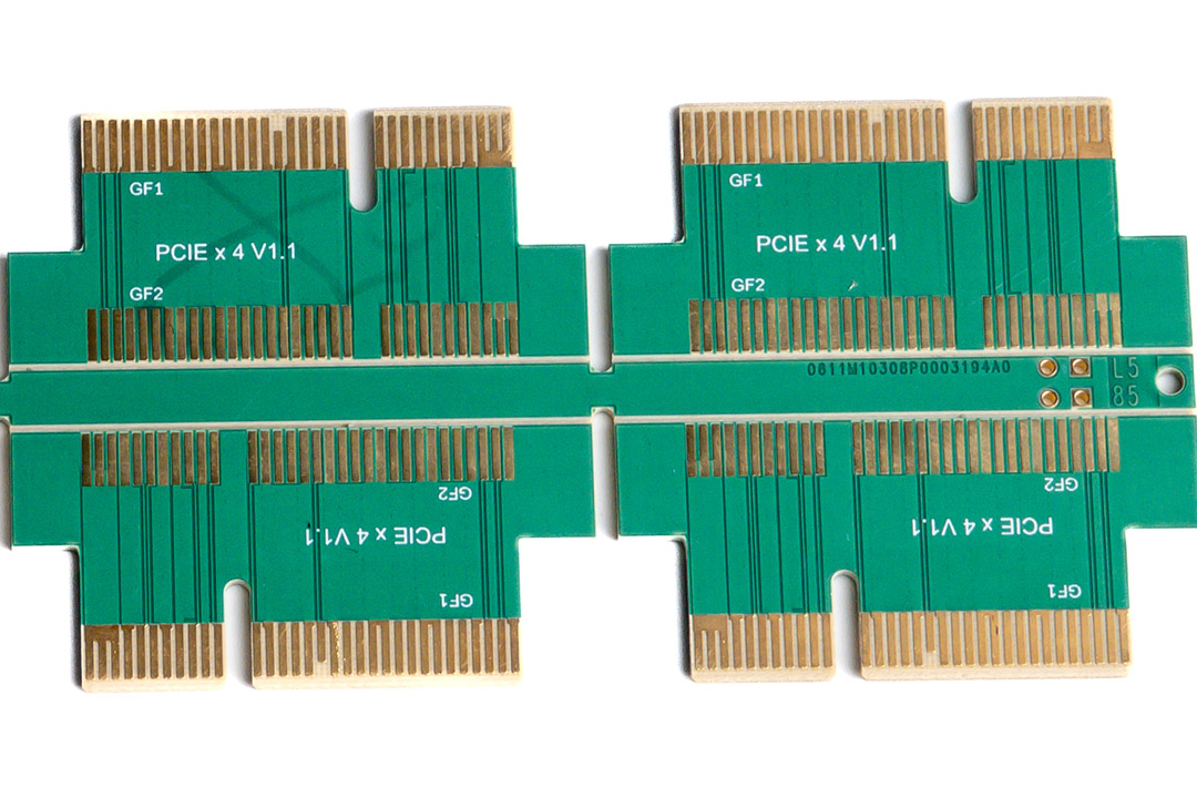
| Finger Placement | Single-sided, double-sided, stepped fingers,Segmented Gold Fingers |
| Beveling Angle | 20° – 60° |
| Beveling Depth | 0.4mm – 2.5mm |
| Beveling Tolerance | ±0.1mm – ±0.05mm |
| Residual Thickness | 0.2mm – 0.5mm |
What is a Gold Finger PCB?

A PCB gold finger refers to the series of gold-plated edge connector pads or contacts located along the edge of a printed circuit board (PCB). These gold fingers are gold-plated connectors that serve as the interface between the PCB and external devices, such as a motherboard, expansion slot, or another circuit board—enabling critical data transfer and electrical connection.
Gold fingers are typically fabricated through a meticulous plating process, incorporating an alloy mixture of electroplating gold—most commonly hard gold—over a nickel barrier atop a cleaned PCB pad surface. The gold layer forms an ultra-flat, durable surface that can withstand the abrasive effects of constant PCB usage, including repeated insertions, removals, and harsh environmental exposure.
PCB gold finger plating thickness and finger length are determined according to connector requirements, intended application, and expected number of insertion/extraction cycles.
A Visual Guide to PCB Gold Fingers
| Layer | Material/Finish | Function |
| Copper Pad | Copper | Conducts electronic signals throughout the board |
| Nickel Layer | Nickel | Prevents copper diffusion, bonds gold uniformly, increases hardness |
| Gold Layer | Hard Gold (alloy) | Provides corrosion resistance, high conductivity, durable contact surface |
Why Are Gold Fingers Used on a Printed Circuit Board?

Gold fingers provide the ultimate solution for edge connector reliability in the most demanding electronic applications. Their role includes:
Why Gold Is Used
Gold is chosen for edge connectors of the PCB because it is:
- Highly Conductive:Ensures minimal signal loss, even at high frequencies
- Resistant to Corrosion:Gold doesn’t oxidize, guaranteeing long-term reliability
- Extremely Wear Resistant:Hard gold can withstand the abrasive effects of thousands of mating cycles
Gold fingers are also incomparable for maintaining low electrical contact resistance throughout the life of the device.
The Application of Gold Fingers
Gold fingers are used in a broad spectrum of electronics and devices, from consumer to industrial to specialized mission-critical hardware. Applications include:
- High-frequency PCBs for servers, 5G base stations, routers.
- DDR4/DDR5 RAM modules.
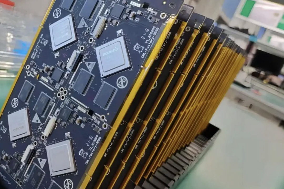
- PCIe, PCI, AGP, and other expansion cards.
- USB, SD, SIM, and proprietary board-to-board connectors.
- Medical devices, automotive ECUs, aerospace modules.
Applications of Gold Finger PCB
Application of PCB gold fingers expands across every vertical:
1. Personal Computers and Servers
- RAM sticks:PCB gold fingers connect memory modules to the motherboard, supporting high data rates and fast RAM upgrades.
- Expansion cards:Network, graphics, sound, and storage cards connect through gold finger edge connectors.
- Hot-swappable server blades:Use hard gold-plated fingers for robust, reliable data center service.
2. Consumer Electronics
- USB flash drives:PCB gold finger pads interact with the host port over many plug cycles.
- Smartphone PCBs:Support module upgrades and rapid signal transmission.
3. Industrial, Medical, and Automotive
- Industrial controllers and sensors:Use gold finger edge connectors for swappable modules.
- Automotive ECUs:Gold fingers withstand vibration, temperature swings, and harsh conditions.
- Medical devices:Gold finger PCBs in imaging equipment guarantee signal integrity in critical environments.
Application Table
| Device/Domain | PCB Gold Finger Application |
| Desktop PC, Server | RAM, PCIe, graphics cards, add-ons |
| Consumer Devices | USB, SD, game cartridges, modular phones |
| Industrial Automation | PLC modules, industrial I/O, process boards |
| Medical/Aerospace | Diagnostic, monitoring, high-reliability systems |
| Automotive | ECU, smart sensors, infotainment |
Design and Manufacturing Process of Gold Finger PCB

Comprehensive Introduction to PCB Gold Finger Design
Good design and manufacturing are the foundation of every robust gold finger. Here’s what you need to know about LHD TECH’S PCB gold finger design:
- Finger width, length, and spacing (pitch) must align with the connector spec and application.
- Avoid vias, stubs, or copper beneath fingers (keep copper-free along the PCB edge).
- Specify beveling (gold finger beveling), usually 30–45° for easy insertion.
Manufacturing Process of Gold Finger PCB
- PCB Layout & Design:Our designer prepares the PCB artwork, calling out pad location, length, width, bevel angle, and required gold finger plating thickness.
- Panelization:Multiple boards are grouped for efficient gold plating and machining.
- Cleaning:The PCB pad surface is carefully cleaned; a cleaned gold finger pad surface is crucial for adhesion.
- Nickel Plating:Nickel is electroplated onto the pads (typically 3–7 μm). This gold finger plating process ensures a barrier that makes gold adhere and protects from copper migration.
- Gold Plating:The actual gold plating process applies hard gold (alloy) to the exposed pads. Gold thickness can be customized (usually 1–5 μm, see gold finger plating thickness below).
- Beveling:The board edge is chamfered—see “gold finger beveling”—to ease mating and reduce mechanical wear.
- No Soldermask/Silkscreen in Gold Finger Area: For optimal contact, the edge of the PCB where gold fingers are applied is kept free from soldermask or silkscreen. This helps maintain a cleaned gold finger pad surface and ensures reliable connections.
- Final Inspection and AOI: Automated Optical Inspection (AOI) and electrical testing confirm the gold finger length, alignment, thickness, and absence of defects per the customer’s design rules of PCB gold fingers.
- Depanelization: The boards are separated from the panel, and any final cleaning or edge polishing is completed. The edge of a PCB is checked to confirm the correct chamfer and absence of burrs or uneven plating.
Gold Finger Plating, Thickness, and Process Details

Plating Process of Gold Fingers
LHD TECH’S plating process for PCB gold finger involves electroplated hard gold, where an alloy mixture of electroplating gold (often a blend of gold and cobalt or nickel) is deposited over the nickel layer. This is a crucial differentiation from ENIG (Electroless Nickel Immersion Gold), which is used for general surface pads but does not provide the same abrasion resistance required for edge connectors of the PCB.
Guide to PCB Gold Finger Plating Thickness
Gold finger plating thickness is a parameter that must be carefully chosen based on the intended application of PCB gold fingers. The thicker the gold, the higher the cost of gold plating, but also the greater the wear resistance and the number of reliable mating cycles.
Typical Plating Thickness Recommendations:
| Application | Gold Thickness (µm) |
| Light use (consumer devices) | 0.76–1.3 |
| Moderate use (office/industrial) | 1.3–2.54 |
| High-cycle (server, telecom) | 2.54–5+ |
Inspection, Testing, and Quality Control for Gold Finger PCB
Inspection & Testing
- AOI (Automated Optical Inspection):Checks every finger for placement, thickness, alignment, and surface defects.
- E-Testing:Confirms continuity and absence of shorts in connector areas.
- Microsection and XRF Analysis:Verifies gold and nickel plating thickness and layer quality.
- Insertion/Extraction Testing:Simulates effects of constant PCB usage cycles.
- Adhesion (Tape) Test:Ensures the gold layer is not easily removed during connector mating.
Appearance Standards
- Clean, scratch-free gold finger surface.
- Plating thickness meets specification along all pads.
- No exposed copper or nickel at finger edge.
Conclusion: Why Learn About LHD TECH’S Gold Finger PCB and Their Future
As connectors, data rates, and product lifespans advance, understanding the ultimate guide to PCB gold fingers empowers engineers, managers, and sourcing professionals to make informed decisions. The gold fingers remain a lynchpin for reliable, upgradeable, and serviceable electronics.
Gold fingers are the gold-plated connectors that form the robust bridge—mechanically and electrically—between a printed circuit board and the system around it. Their design, plating thickness, and manufacturing process drive the entire capability of modular, high-speed, and upgradeable technology.