


Introduction to High Frequency PCB: Demand, Evolution, and LHD PCB

Modern electronic equipment fundamentally relies on operational speed. High-frequency and high-speed data transmission have now become essential requirements across a wide range of application fields, including 5G communications, radar systems, the Internet of Things, and microwave communications. To meet these demands, the market has generated an unprecedented need for reliable, high-performance high-frequency PCB solutions, which must be capable of supporting complex signal processing at continuously increasing transmission rates.
High-frequency PCBs, also referred to as HF printed circuit boards, are specifically designed for high-frequency circuit applications. Their primary objective is to maintain superior signal integrity even when circuits operate at high speeds. Typically, the operating frequency range of such PCBs spans from 500 MHz to several tens of gigahertz. This frequency band is fundamental to achieving low-loss and distortion-free signal transmission.
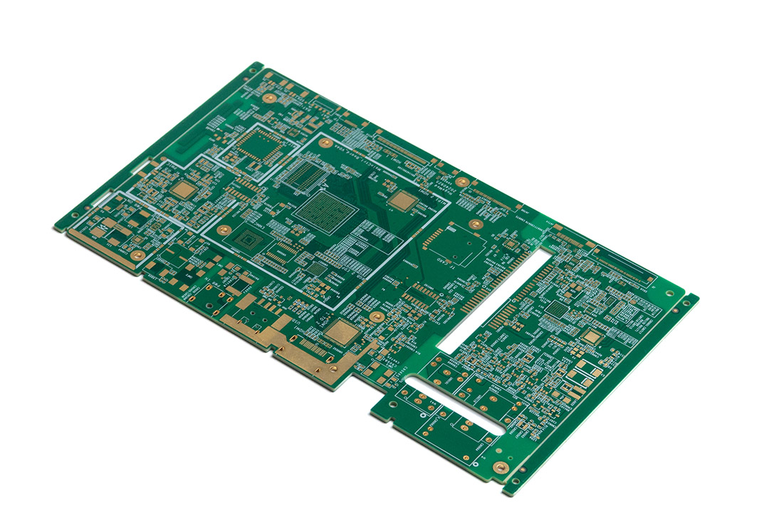
LHDPCB is a top-tier printed circuit board (PCB) manufacturer in China. The company possesses solid professional expertise in the design of high-speed and high-frequency PCBs, selection of relevant materials, and assembly of high-end products, and serves leading enterprises across various industries worldwide. LHDPCB utilizes the most cutting-edge PCB design software currently available and continuously optimizes its own manufacturing processes. For various complex PCB design tasks and challenges encountered during the manufacturing process, the company provides professional technical support solutions. Thus, LHDPCB has become the preferred cooperation partner for numerous innovative enterprises worldwide in PCB-related collaborations.
What Makes a High Frequency PCB?
The core definition of high-frequency PCBs lies in their ability to support specific operating frequencies—a performance level that far exceeds what traditional PCB materials and layout designs can achieve. This characteristic is of critical importance for RF circuits, microwave modules, high-speed PCBs, and all printed circuit designs that need to operate in the gigahertz range or even higher frequency bands.
Typical Frequency Ranges
| Type of PCB | Frequency Range | Applications |
| Standard Digital PCBs (FR-4) | <1 GHz | Consumer, low-speed digital |
| High-Speed PCBs | 1–5 GHz | High-speed data (DDR, USB) |
| High Frequency PCB / HF PCB | >500 MHz up to 100+ GHz | RF/microwave, 5G, radar |
| High-Speed and High-Frequency PCBs | >5 GHz–mmWave | Satellite, mmWave |
High frequencies emphasize not just speed, but also purity of transmission in every inch of board real estate. For a high frequency board, impedance control, the number of vias in high-frequency signal paths, and optimized PCB layout are all critical.
Characteristics of High Frequency PCBs
The design of high-frequency PCBs follows the industry’s fundamental principles, while their performance differentiation from conventional circuit boards primarily stems from three core elements: the selection of specialized substrates, the implementation of precise geometric structures, and the application of advanced manufacturing processes. The key characteristics of this type of circuit board are specifically reflected in the following aspects:
- Stable Dielectric Constant:Lower and more consistent Dk (as opposed to relatively high dielectric constant materials in standard boards).
- Low Loss Factor (Df):Minimizing signal energy loss, critical for performance at high frequencies.
- Thermal Stability:Excellent dimensional and material stability across temperature ranges.
- Moisture Resistance:Prevents shifts in dielectric and losses across different climates and humidity levels.
- Advanced PCB materials:Materials like PTFE (Teflon), Rogers PCB, Taconic, and Isola ensure robust handling of high-frequency signals.
Summary Table: Characteristics of High-Frequency PCBs
| Characteristic | Importance | How Achieved |
| Dielectric Constant | Controls signal velocity & impedance | Rogers, PTFE, low-Dk materials |
| Loss Tangent (Df) | Reduces signal attenuation at high frequency | Advanced HF PCB laminates |
| EMC/EMI Suppression | Lessens interference between signals | Ground planes, via fences |
| Moisture Resistance | Ensures consistent values in changing environments | Materials used: low absorption |
| Thermal Conductivity | Withstands high-speed and high-frequency heating | PCB material with high CTE |
| Precision PCB Design | Guarantees performance at high frequencies | PCB layout, stackup, trace geometry |
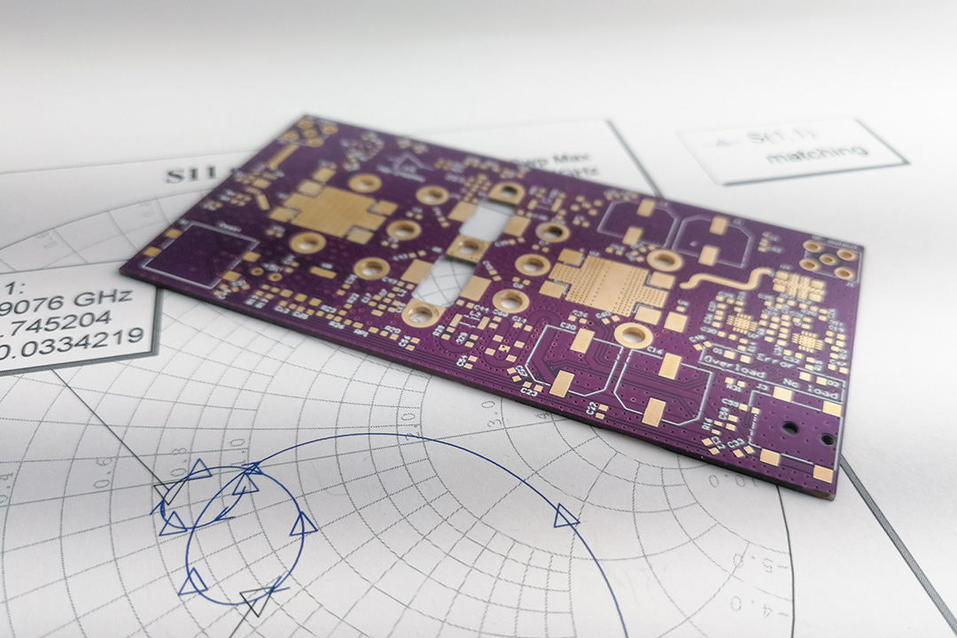
High Frequency PCB Materials: Properties and Selection

Why Material Selection Matters in High-Frequency PCBs
High frequency PCB design starts with the right PCB material. At high frequencies, materials have lower dielectric constants, minimal loss tangent, and high purity to maintain signal integrity.
Materials Used in HF PCBs
- Rogers PCB:A global standard for high-frequency materials; offers low Dk and Df for frequencies up to 40+ GHz.
- PTFE (Teflon):Excellent for microwave, radar, and aerospace—best for high-frequency circuit boards.
- Taconic, Isola, Panasonic Megtron6:Chosen for their blend of affordability, low loss, and process compatibility.
- Advanced Laminates:Rogers 4003C, 4350B, RO3003, Taconic RF-35, Isola IS680 AG.
Material Comparison Table
| Material | Dk (@10GHz) | Df (@10GHz) | Frequency Handling | Key Application |
| Rogers 4350B | 3.48 | 0.0037 | 40+ GHz | 5G, radar, aerospace |
| PTFE (Teflon) | 2.20–2.60 | 0.0009–0.0025 | 60+ GHz | Microwave, satellite, radar |
| Panasonic Megtron6 | 3.5 | 0.0020 | 20–40 GHz | Automotive, telecom |
| FR-4 | 4.2–4.8 | 0.019–0.025 | <3 GHz | Low/mid-speed digital |
Design Considerations for High Frequency PCB Design
Critical Steps in High-Frequency PCB Design
Design of PCB for high frequencies is more demanding than standard boards. Here’s what makes a great high-frequency PCB design:
PCB Layout & Routing
- Keep traces as short as possible; longer routes increase loss and delay.
- Maintain impedance control via consistent trace width and ground referencing.
- Avoid right-angle bends (use 45° or curves); sharp bends reflect high frequency signals.
- In high-frequency circuit design, engineers must strictly control the number of vias. This practice serves as a fundamental measure to ensure signal integrity. Excessive vias placed along high-frequency signal paths can introduce considerable parasitic inductance. Such parasitic inductance may subsequently give rise to signal reflection, thereby compromising the overall performance of the circuit.
- Use multilayer structures with tightly coupled power/ground planes.
- Ensure robust shielding and separation for analog/RF and digital signal regions.
Component Placement and Decoupling
- Place decoupling capacitors close to ICs—high-speed and high-frequency PCB designs need high-frequency decoupling capacitors to reduce noise.
- Isolate noisy clock sources and digital lines from RF-sensitive areas.
Simulation and Validation
- Use PCB design software with electromagnetic field solvers to predict and verify signal quality and loss before prototyping.
Checklist for HF PCB Design
- Material selection supports intended frequency range.
- Controlled impedance traces for all RF paths.
- High-frequency decoupling near fast ICs.
- Signal integrity simulation conducted before layout sign-off.
High-Frequency Applications: Where High Frequency PCBs Deliver
High-frequency PCBs are crucial in systems where high speed and high frequency signal transmission is non-negotiable. The variety of applications they serve is a testament to their versatility and importance in modern electronics.
Key High-Frequency Applications
- Wireless Communication (5G, WiFi, Bluetooth):High frequency PCBs handle high-speed data transmission in all wireless base stations, antennas, IoT devices, and mobile infrastructure.
- Radar and Aerospace:High-frequency printed circuit boards are essential for radar systems, aerospace navigation, and defense applications, where operating frequencies may stretch into the millimeter-wave range.
- Medical Technology:Advanced imaging systems (MRI, ultrasound, wireless patient monitors) utilize high-frequency PCB designs for noise immunity and precision.
- Automotive Electronics:Advanced Driver Assistance Systems (ADAS), car-to-car communication, and automotive radar all demand high-speed and high-frequency PCBs.
- Satellite Systems and Microwave Transmission:Satellites and ground stations rely on HF PCBs for signal clarity over vast distances and resistance to environmental stress.
Manufacturing and Quality Testing in LHD TECH’S High-Frequency PCB Design

LHD TECH’S High frequency PCB manufacturing is all about meticulous process control, material purity, and validation at every step.
LHD TECH’S Design and Manufacturing Workflow
- Material Selection:Choose high-frequency PCB laminates with low Dk/Df for the targeted frequency.
- PCB Layout:Leverage PCB design software for detailed stackup, controlled impedance, and minimal vias in high-frequency paths.
- Lamination and Etching:Employ precision equipment to ensure layer alignment and clean feature definition.
- Drilling:Use laser drilling for HDI; X-ray guidance ensures via quality even in multilayer high-frequency boards.
- Electroplating:Deposits uniform copper layers; critical for high-speed and high-frequency circuits.
- Solder Mask and Final Finish:Provides environmental protection; options like ENIG are favored for high-frequency applications.
- Quality Inspection:100% AOI inspection, E-Test for opens/shorts, flying probe on prototypes, and S-parameter/TDR testing for high performance at high frequencies.
Common Design Challenges and Solutions
Typical HF PCB Problems (and Solutions)
- Signal Loss / Reflection:Use low-loss high-frequency PCB materials, optimize trace impedance, and minimize the number of vias in high-frequency signal lines.
- Impedance Mismatch:Thorough impedance calculation, stackup validation, and simulation with specialized PCB design software.
- EMC/EMI Issues: Isolate grounds, use guard traces, design with via fences, and maintain separate analog and digital domains.
- Thermal Instability:Choose materials with high thermal conductivity and low CTE; ensure even copper distribution for better heat dissipation.
- Moisture Absorption:Specify high frequency PCB materials (like PTFE or Rogers PCB) for environments with humidity or condensation.
Advantages of High Frequency PCBs

The advantages of high-frequency PCBs go far beyond supporting faster signals:
- Exceptional Signal Integrity:Low loss and distortion in high-frequency circuits assure optimal function in high-performance RF equipment.
- High-Speed Data Transmission:Enabling the backbone of 5G, IoT, satellite, and radar advancements.
- Reliability in Demanding Conditions:Materials and process deliver performance at high frequencies under humidity, vibration, and temperature extremes.
- Precision and Miniaturization:Suitable for shrinking device footprints while maintaining or increasing performance.
- EMC/EMI Compliance:Better suppression of noise and interference through grounded and shielded layouts.
- Design Flexibility:LHD TECH’S HF PCBs can be customized for hybrid digital/analog systems and a wide variety of applications.
Conclusion: Mastering High-Frequency PCB Design with LHD PCB
High frequency PCB design is the gateway to unlocking reliable, high-speed and high-frequency electronic systems. The right choices in PCB material, stackup, and layout translate to real-world advantages in signal integrity, performance, and durability. Today’s advanced world requires high-frequency PCBs that can handle the ever-rising demand for frequency, speed, and complexity in printed circuit boards.
LHDPCB stands ready to help you realize your next breakthrough—offering global best-practice in design, material selection, and manufacturing.
- Contact LHDPCB today for expert engineering advice, rapid prototyping, and production in the most demanding high frequency PCB and high-speed PCB.
- Your next innovation deserves nothing less than a board that’s truly built for the future of signal and speed.