Introduction
In today’s electronics manufacturing industry, surface mount technology (SMT) and high-precision PCB assembly have become the cornerstones for achieving product performance and reliability. As one of the core reflow soldering processes reflow soldering directly determines the final quality and service life of various electronic products, ranging from smartphones to medical devices. A profound understanding of the temperature curve setting for reflow soldering, the correct operation of the reflow soldering furnace, as well as the scientific handling methods of solder paste, components and PCBS is the key to ensuring firm solder joints and outstanding product performance.
As a professional brand in the field of SMT soldering technology, LHD TECH is always committed to providing customers with efficient and stable reflow soldering solutions. This article will systematically analyze each link of the reflow soldering process, covering a detailed analysis of each process stage, the core role of temperature profile, the characteristics of different reflow soldering techniques, and how to achieve high-quality solder joints in actual production. Whether you are a novice just getting started with PCB assembly or a professional looking to further enhance your craftsmanship, LHD TECH will provide you with in-depth yet easy-to-understand technical guidance and practical suggestions from a professional perspective, helping you achieve better results in the electronic assembly process.
Overview of Reflow Soldering and Its Importance
In simple terms, reflow soldering is a process that precisely controls heating to firmly solder surface mount components onto the printed circuit board (PCB). Wave soldering merely allows molten solder to touch the bottom of the board, while reflow soldering uses a reflow oven, subjecting the entire assembled board to a pre-designed and highly precise heating process. This process will melt the pre-printed solder paste, moisten the PCB pads and component on the PCB, and then cool down to solidify again, forming a strong and reliable connection.
The reflow process has formed the current SMT (Surface Mount Technology). It enables electronic engineers to add more performance per square millimeter of printed circuit board, and the repeatability of this process is particularly high. Whether it is for sample trial production or large-scale mass production, it relies on it to ensure the consistency of quality.
Principles of Reflow Soldering
At its core, the principles of reflow soldering focus on:
- In the process of consistent solder paste, it is essential to ensure that the amount of solder paste on each PCB pad is precise and consistent. An appropriate amount of solder paste is the foundation for the quality of subsequent soldering.
- When mounting components, first component placement them on the board. Either hand pick and place machine is acceptable. Make sure the components are placed upright and pressed steadily to ensure perfect contact between the component pins and the solder paste.
- When reflow soldering passes through the furnace, first set reflow oven temperature profile for “heating, melting and cooling” for the furnace. Let the molten solder heat up evenly first, melt smoothly after reaching its melting point, and ensure that the molten solder fully penetrates the pads and pins. Finally, cool it down quickly to stabilize the solder joints.
A well-designed temperature profile is the key to the overall soldering quality. It directly determines the welding effect and avoids a bunch of troubles at the same time – such as components being damaged by thermal shock, solder paste not wetting properly leading to false soldering, or the surface of the solder joint turning gray and rough.
Types of Soldering: Reflow Solder vs. Wave Soldering
Reflow Solder
- Uses reflow soldering equipment (mainly a reflow oven with zones for preheat, soak, reflow, and cooling).
- Ideal for surface mount devices and high-density PCB assemblies.
- Controlled thermal profiles mean minimal damage to the board or components.
Wave Soldering
- Floods the underside of the printed circuit board with a wave of molten solder.
- More common in through-hole assembly or single-sided PCB assemblies.
- Not suitable for most SMT layouts due to potential for bridging/flooding fine-pitch devices.
Key Differences:
| Factor | Reflow Soldering | Wave Soldering |
| Best for | Surface mount (SMT) | Through-hole components |
| Control process | Temperature profile | Solder wave speed/temp |
| Solder phase | Melts then solidifies | Immediate contact |
| Defect profile | Tombstones, voids | Bridges, icicles |
The Reflow Soldering Process: Step-by-Step
The reflow soldering process consists of multiple key stages:
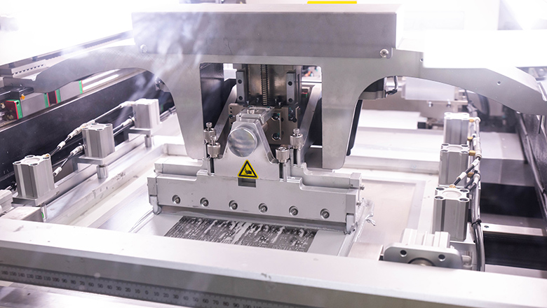
1. Solder Paste Application
- Solder paste (with flux) is deposited onto PCB pads using a stencil. The quality, volume, and location of the paste impact individual joints.
- Consistent solder paste volume ensures even melt the solder paste action and avoids excessive solder paste (which leads to bridging).
2. Component Placement
- This step involves surface mount components onto the board. Whether using a pick and place machine or manual soldering, the core lies in two points: precise alignment, ensuring that the component pins precisely land on the solder paste of the pads. Hold your hand steadily and do not move it or rub it against the solder paste.
3. Preheat Zone
- This first stage of the reflow after the board enters the furnace, and the temperature needs to rise gradually. There are two purposes: one is to allow the solvent in the solder paste to evaporate gently; The second is to provide a buffer for the entire board and components to prevent thermal shock.
4. Soak or Dwell Temperature
- At this soak stage, the temperature needs to be maintained constant to ensure that each large component and small capacitor on the entire PCB board is evenly exposed to the uniform temperature. At this point, the flux in the solder paste starts to work, cleaning the oxide layer on the pads and component pins thoroughly, preparing for the subsequent soldering.
5. Reflow Zone (Peak Temperature)
- This is the core of the entire reflow zone. Itrises to maximum/reflow temperature, and the solder paste melts into liquid solder in this area, soaking onto the pads and pins, thus forming solder joints.
- Note: The temperature is not the higher the better, notis the reflow time the longer the better. If the reflow oven temperature profile is too high or the components stay in this high-temperature zone for too long, they may burn out and the surface of the solder joints will become rough and gray, like sand.
6. Cooling Zone
- The solder joints have formed and need to be quickly shaped. The cooling zone down the temperature at a controllable rate avoid thermal shock or cracking, allowing the molten solder to solidify into a firm solder joint.
- The temperature should drop at a steady pace. If it drops too quickly, the components and solder joints will generate internal stress due to severe contraction, leading to cracks or thermal shock. Only a smooth cooling process can ensure that each weld point is both strong and conductive.
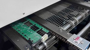
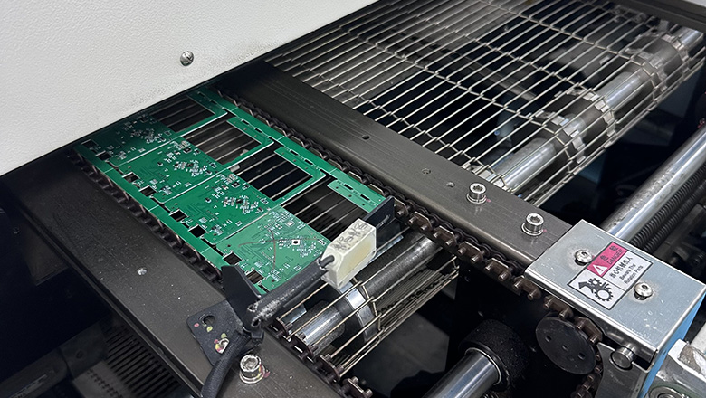
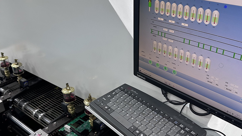
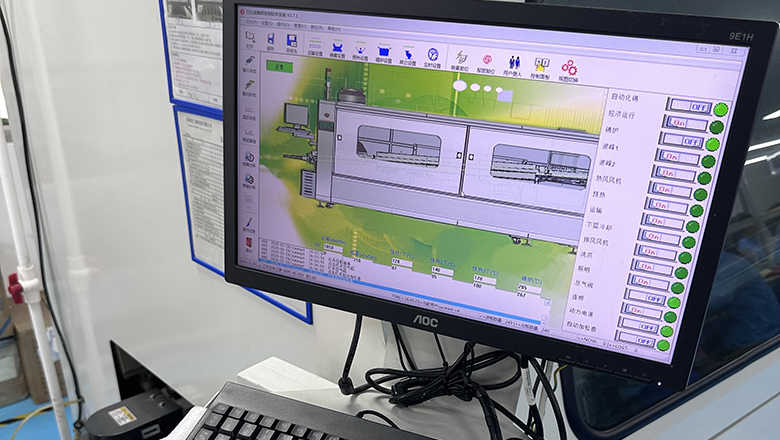
Reflow Soldering Equipment: Ovens, Pick-and-Place, and More
The right reflow soldering equipment determines the quality and efficiency of your PCB assemblies.
Types of Reflow Ovens
- Hot Air/Convection Ovens: Use moving air for even heating.
- Infrared Ovens: Direct heat, less common in modern assembly.
- Nitrogen Reflow Ovens: Lower oxidation, better for lead-free solder and fine-pitch components.
- Vapour Phase Ovens: Use boiling liquid vapor for perfect uniform temperature.
Critical Factors:
- Number of temperature zones.
- Precision of temperature control for each stage of the profile.
- Compatibility with your chosen type of solder.
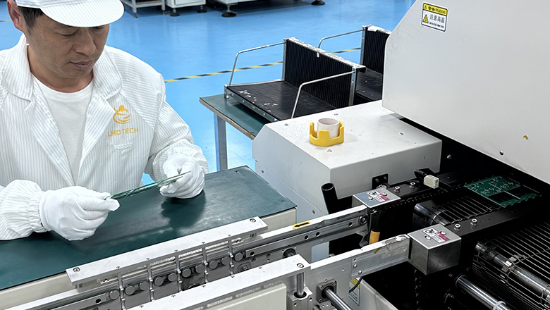
Pick and Place Machines
- Automate component placement with high speed and accuracy.
- Use software-defined programs for repeatable, large-scale production.
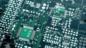
PCB Design and Materials for Reflow Soldering
Designing for the Reflow Process
- Pad size, spacing, and orientation are crucial for correct wetting and to minimize soldering defects.
- Use design practices that account for thermal profile and copper balancing to ensure even heating.
- Proper PCB stackup (number of layers and copper distribution) helps minimize temperature variation in the reflow oven.
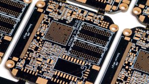
Choosing the Right Materials
How to choose PCB substrate?
- FR-4 is the one we use most frequently. It has stable performance and an affordable price, and can handle the vast majority of situations. But it is not the first choice in lead-free welding situations.
Which surface treatment for solder pads is better?
- ENIG (Gold plating) : High-end craftsmanship, smooth surface, strong anti-oxidation ability, but slightly higher cost.
- OSP (Organic Solder Mask) : It coats the pads with a “transparent protective film”, which is low-cost and environmentally friendly, but the protective film is not heat-resistant and is prone to scratches.
- HASL (Tin spraying) : This is a relatively traditional process. It uses hot air to flatten the molten tin-lead alloy. It has good solderability and is relatively inexpensive, but its surface flatness is slightly poor and it is not very suitable for components with fine pitches.
Preparing and Applying Solder Paste
Solder Paste Selection
- According to the solder paste data sheet, refer to the recommended temperature range and profile. This is the best range that has been tested and verified. It is the safest to follow it.
The selection of solder paste should be matched based on the actual situation of the product:
- Environmental protection requirements: Choose lead-free and lead-containing solder paste.
- Component type: Select solder pastes with different popularity, alloy composition and melting points.
- Temperature resistance requirements: Different heat-sensitive devices.
Paste Application Best Practices
- Consistent solder paste: The quality of each solder joint is determined at the moment of solder paste printing. It is necessary to use a calibrated printing press and regularly check the solder paste volume and thickness of the solder paste to ensure that each print is consistent with the parameters recommended by the solder paste datasheet.
- The amount of solder paste used: If excessive solder paste is printed, it is prone to “overflow” during reflow, causing a bridging short circuit. The print is too little, and the surface mount components. cannot be connected, resulting in a false soldering and open circuit directly.
- Environmental control: If the temperature and humidity in the workshop fluctuate, the solvent will evaporate prematurely. Therefore, the printing operation must be carried out in an environment with controlled temperature and humidity to provide a stable working state for the applying solder paste.
Temperature Profiles and the Reflow Oven
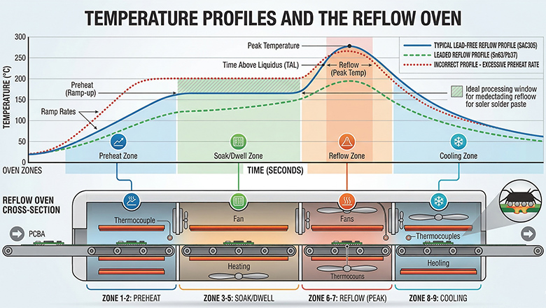
We are well aware that a well-designed temperature profile is a core process parameter for ensuring the reliability of reflow soldering. This temperature profile – often referred to as the thermal profile or reflow profile – precisely describes the dynamic trajectory of the PCB’s temperature over time as it moves in the reflow oven.
Importance of Temperature Profile
This curve is not a fixed and universal template, but needs to be customized for each PCB model. The main considerations are as follows:
- The characteristics of solder paste type: Solder pastes of different brands and with different alloy compositions have different requirements for temperature.
- The size of the board: The board is thick, the components are large, and it absorbs heat, so the temperature needs to be increased. Where the board is thin and the components are small, overheating must be prevented.
- The performance of the equipment: The heating method and heat transfer efficiency of the reflow oven also determine how the curve should be adjusted.
The temperature profile is essential for prevent components from being subjected to thermal shock due to sudden temperature changes, making the entire welding process gentler and more stable.
Types of Reflow Profiles
- Ramp-Soak-Spike (RSS): This is a common approach: First, gently heat up to allow the board to adapt; Then enter the insulation zone to allow the temperature and flux activity to reach the optimal state; Then quickly sprint to the peak temperature to complete the welding; Finally, control the cooling.
- Ramp-to-Spike: This is relatively straightforward and forceful. It does not have a heat preservation zone and directly heats up to the peak. The advantage is that the process is short and the efficiency is high. However, because it lacks temperature buffering, it is usually only used on single-sided boards with simple structures and single components.
- Double-sided profile: The common practice is to run the reflow soldering twice, but the curve for each side needs to be designed separately. For instance, solder the side with fewer components and higher temperature resistance first. Once it is soldered, solder the other side. Control the temperature to prevent the already soldered side from melting again and causing the components to fall off.
Typical Reflow Profile Table
| Zone | Temperature Range | Duration | Purpose |
| Preheat | 25°C – 150°C | 60–120s | Safely raises PCB and components to avoid thermal shock |
| Soak (Dwell) | 150°C – 190°C | 70–120s | Ensures uniform temperature and activates flux |
| Reflow (Peak) | 230°C – 250°C* | 20–40s | Solder paste melts, forms molten solder, wets joints |
| Cooling | 250°C – 50°C | 60–120s | Solidifies joints, prevents cracks and grainy solidification |
Key Zones: Preheat, Soak, Reflow, and Cooling
Each zone in the reflow process serves a targeted purpose:
Preheat Zone (First Stage of the Reflow)
- Raises temperature of both components and the PCB gently to prevent thermal shock.
- Allows solvents in the solder paste to evaporate, reducing voids and splatter.
Soak or Dwell Zone
- Maintains a steady temperature to reach a uniform temperature across the assembly.
- Fully activates flux in the solder paste, cleaning metal surfaces for optimal wetting.
- Begins softening the solder paste, preparing to reach point of the solder paste(liquidus).
Reflow Zone (Peak)
In the view of LHD TECH, there are two key points for controlling the return zone:
- The temperature should be appropriate: The peak temperature must first step is ensure the melt the solder paste, allowing the molten solder to fully soak the pads and pins, forming a firm solder joint. However, this maximum temperature should be based on the component with the minimum tolerance limit.
- The timing must be accurate: After the solderpaste melts, the time it stays in this temperature zone at the reflow phase should be controlled. The time is too short, the wetting is not sufficient, and the solder joints are weak. Over time, the components may be damaged.
Cooling Zone
- Controls temperature drops so solder joints solidify safely.
- Fast cooling can induce stress/cracking; too slow cool-down can create large grain structure and reduce joint strength.
- Temperature profile for cooling is just as important for ensuring the final mechanical/electrical properties.
Best Practices for High-Quality Solder Joints
Sustaining premium soldering results, especially with complicated or fragile assemblies, depends on following industry best practices at every stage.
Before Reflow
- Use only IPC-compliant, moisture-controlled components and PCB.
- Match the type of solder and paste to component finishes (e.g., lead-free, HASL, OSP).
- Log all production variables, from lot codes to process parameters.
During Reflow
- Monitor process parameters live, not just setpoints—watch for actual temperature of the PCB assembly.
- Use profiles tailored to every new assembly, not a “one-size-fits-all” approach.
- Document any adjustments or changes—especially when switching solder paste, pcb assemblies, or profile.
After Reflow
- Inspect every joint—automated optical inspection, X-ray for BGAs, and manual review.
- Record defects and corrections to iterate improvements for the next run.
Common Defects and Solutions
Despite all precautions, certain problems regularly occur in PCB reflow:
| Defect | Cause | Solution |
| Solder Bridging | Excess paste, fine pitch, too hot at reflow | Reduce volume, optimize profile, tweak stencil |
| Tombstoning | Thermal imbalance, uneven paste | Balance copper, fine-tune temperature ramp and soak |
| Cold Joints | Underheating, poor wetting | Increase reflow temp/time, clean surfaces, check flux |
| Voids/Pinholes | Solvent entrapment, excessive ramp rate | Slow ramp rate, use recommended paste, control environment |
| Insufficient Solder | Small aperture, not enough paste | Resize stencil apertures, check print process |
Troubleshooting Insight:
The core root causes of common soldering defects in surface mount PCB assembly can often be attributed to the loss of control over three key links: improper design of temperature profile, oversight in solder paste process management, or insufficient consideration at the beginning of PCB design.
Safety, Inspection, and Environmental Concerns
Safety Procedures
- During the reflow oven soldering process, chemical substances such as flux in the solder paste can volatilize due to heat, which is harmful to human health. When the equipment is in operation, it is necessary to ensure that the exhaust and smoke exhaust system is working properly to keep the air in the workshop circulating.
- Whether adjusting solder paste or using chemical cleaners, protective gloves and goggles should be worn. If these solvents in the solder paste come into direct contact with the skin or splash into the eyes.
- Discard cleaning waste, excess or expired paste, and empty flux packaging per regulatory standards.
Inspection Best Practices
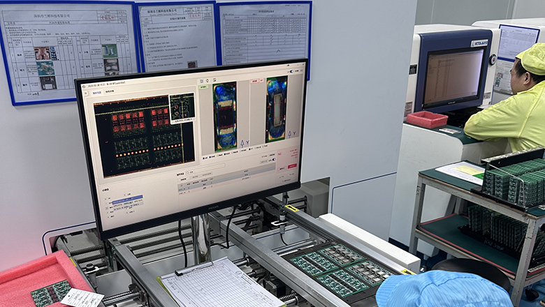
- Automatic optical inspection is the most efficient. It can quickly detect component offset, monument erection, and bridging, ensuring that problems do not flow into the next stage.
- If there are chips like BGA with solder pads hidden at the bottom of the components on the board, X-ray is needed to “see through” them to check if there are any voids, Bridges or open solder joints on the solder balls.
- In sample trial production or small-batch production, experienced technicians conduct manual inspections under microscopes, which is more flexible and meticulous.
Environment
- Actively responding to global environmental protection trends such as the RoHS Directive, we comprehensively adopt lead-free solder. Not only does it meet the regulatory requirements, but it can also create a safer and cleaner working environment for the production workshop.
- When using equipment such as nitrogen gas shielded welding or vapour phase ovens, we pay special attention to the recovery and recycling of media such as nitrogen and special working fluids. Save costs, respect resources and reduce pollution.
- Strictly monitor the exhaust system of each reflow oven in the workshop and regularly test the air quality. Ensure that all emissions comply with safety and environmental protection standards.
Frequently Asked Questions
Q: Why is the temperature profile so important in reflow soldering?
A: The temperature curve directly determines the forming quality of each solder joint. Insufficient or excessive heating can lead to a series of defects such as cold welding, poor wetting and even pad peeling. A precisely controlled curve can ensure that the solder melts evenly and wets thoroughly, and then form a reliable solder joint with both mechanical strength and electrical conductivity after cooling.
Q: What’s the difference between lead-free and leaded solder pastes?
A: The peak temperature of lead-free solder paste represented by SAC305 usually needs to reach 235-250°C, which is much higher than that of lead-containing processes. At the same time, the flux activity system is also completely different. Therefore, before adjusting the parameters, it is essential to strictly refer to the technical specification sheet provided by the solder paste manufacturer.
Q: How do you deal with double-sided assembly in an SMT process?
A: When welding double-sided boards, it is recommended to weld the side with heavier or more components first. For the bottom components that may shift during the second pass through the furnace, the red glue dispensing process can be adopted for reinforcement. At the same time, the secondary reflow curve needs to be adjusted specifically to minimize the thermal shock to the solder joint on the already soldered side as much as possible.
Q: What’s the best way to avoid thermal shock?
A: In the design of temperature curves, mild heating and cooling slopes should be adopted. At the same time, for moisture-sensitive components, they must be thoroughly pre-baked before mounting in accordance with their MSL grade to prevent the “popcorn” phenomenon.
Q: When should you use reflow soldering instead of wave soldering?
A: Reflow soldering is suitable for all surface mount components and mixed boards with a small number of through-hole components, and can individual joints with a hot air/infrared control for each solder joint. Wave soldering, on the other hand, should be reserved specifically for handling board types that mainly consist of through-hole components or have an extremely low proportion of mixed components, in order to maximize the advantages of each process.
Conclusion: Mastering the Reflow Soldering Process
In today’s electronic manufacturing field, a thorough understanding and precise mastery of the reflow soldering process – including the scientific design of temperature curves, the meticulous control of solder paste printing, and the accurate setting of reflow soldering furnaces – is a compulsory course for every printed circuit board (PCB) assembly practitioner.
LHD TECH has always believed that the perfect reflow soldering process is essentially the art of balancing scientific principles and practical experience. A meticulously crafted (carefully designed) temperature profile is at the core of achieving outstanding welding quality. Whether you are dealing with cutting-edge precision surface mount components or conventional printed circuit board assemblies, a profound understanding of how the various temperature zones in the reflow oven—preheat, soak, reflow zone, and the cooling zone – affect the thermal profile and the final quality of each solder joint is a professional yardstick for measuring an outstanding engineer or technician.
Please do remember that even with the most advanced reflow soldering equipment and the most precise surface mount technology (SMT) pick and place machine, if the scientific design of the reflow curve is neglected or there are omissions in the selection of PCBS and solder, everything will return to zero. LHD TECH emphasizes that your entire process flow – from choosing the right type of solder and solder paste, to printing the paste onto the PCB with precise volume, and to strictly controlling each stage of reflow process – must be a closely linked and harmoniously unified whole. Every step needs to be precisely controlled and monitored in real time.
Therefore, our best practice recommendations are: continuous monitoring, frequent adjustments, and always adhering to the solder paste datasheet. Repeatedly verify the recommended optimal temperature range, the critical peak temperature, and the maximum temperature that the components can withstand. Only in this way can common defects such as cold soldering, bridging, and thermal stress be effectively avoided, especially when dealing with high-performance or high-density assembled products, ensuring that each PCB meets the reliable quality standards of LHD TECH.
As you gain experience, you will see that fine-tuning the temperature profile is not a one-time event but a cycle of optimization—especially when component types, board designs, or selected solder paste types change. Even small modifications can have a major impact on results, especially as assemblies grow in complexity and value.
For the sustainability of your assembly line and to ensure compliance in every project, always properly handle all solvents in the solder paste, operate your reflow oven with the correct profiles, and maintain accurate documents for every lot and run. This attention to detail is what differentiates a novice shop from a truly world-class assembly operation.
In summary:
- Understand the process: Know each step of the reflow soldering process—the stages, the role of the reflow oven, best practices for applying solder paste, and correct material handling.
- Design for success: Use DFM strategies for your printed circuit, carefully choose pcb materials, and ensure surface finishes favor the best reflow soldering results.
- Master temperature control: Build and validate a profile tailored to your board and components and the PCB every time you start a new assembly.
- Invest in quality: Prioritize the right reflow soldering equipment, maintain clean stencils, and use only high-grade, consistent solder paste and components.
- Never stop learning: Incorporate feedback from every build, utilize AOI and inspection data, and keep updating your process based on the latest research, best practices, and equipment.
Ready to put these lessons into practice?
Start by reviewing your next reflow profile and tuning each parameter for excellence—because true quality in electronics always begins with mastering the reflow soldering process.