Introduction: Smart Grids, PCBs, and the Modern Energy Revolution
At LHD TECH, we are deeply aware of the advent of the AI era. Currently, the greatest challenge lies in the basic power infrastructure, and the rise of the global smart grid is also becoming a decisive moment for the energy industry. Unlike traditional power grids, smart grids rely on digital technology, advanced communication modules and intelligent control systems to achieve real-time monitoring, optimized power transmission and significant energy efficiency improvements. Nowadays, users can greater control over their energy consumption, and behind this lies the possibility bestowed by the continuous evolution of PCB technology in smart grid systems.
At the core of every efficient and smart grid, PCB (Printed Circuit Board) is indispensable – a key technology that silently carries out power management, data routing, and reliable communication among various grid components. Whether it is supporting distributed generation from renewable energy sources like solar and wind power, optimizing high-power power transmission, or achieving seamless smart grid communication, the importance of PCB assemblies and their materials in the development of smart grids has never been as prominent as it is today.
As a leading provider of smart grid PCB solutions, LHD TECH offers you this ultimate guide, covering everything you need to know in smart grid PCB design: From core design strategies, real-world practical cases, to innovative PCB solutions, and the significance of advanced PCB material selection for building stable, scalable, and future-oriented power grid operations.
PCBs for Smart Grids: The Backbone of Advanced Energy Systems
What are PCBs, and why do Smart Grids need them?
A printed circuit board (PCB) is a thin structural component formed by alternately laminating conductive copper foil circuits and insulating dielectric substrates. In asmart grid system, PCBS form the physical and electrical basis of almost all key grid components- including smart meters, protection relays, power inverters, control panels, and communication gateways. They not only ensure power integrity under different load conditions, but also are responsible for the orderly scheduling of high-speed data streams, the connection with distributed sensor networks, and the bridging between the analog front-end system and the digital control unit in the power grid.
How PCBs Optimize the Smart Grid System
- Power Distribution Systems: PCB undertakes the functions of carrying high-power signals, path guidance and electrical isolation, and is the core link for achieving full-domain power flow regulation and power outage defense in the power grid. Key points for achieving high-power PCB technology: copper thickness and current-carrying capacity, electrical clearance and creepage distance, thermal management design, high-reliability interconnection, and insulation technology.
- Communication between Grid Components: PCB provides an integrated platform for wired and wireless communication modules (modular integration, signal integrity, EM/EMC optimization, PLC coupling circuits), thereby achieving technology to monitor and precise control of the power grid operation status, significantly enhancing the seamless and efficient performance of the energy efficiency management system.
- Digital Control Systems: In the smart grid architecture, multi-core PCBS are isolated from transformers by relying on the commonly used Ethernet PHY of SCADA. AMI involves RF front-end and ADC sampling circuits; The PLC needs to integrate protocols such as the analog front end (AFE) and filter networks to support real-time communication and control instruction issuance.
- Renewable Integration: For the efficient access of solar and wind energy, specialized topological designs such as high-frequency PCBS and multi-layer PCBS (high-frequency PCB, multilayer PCB structure optimization, thermoelectric co-design, electromagnetic compatibility) have become key enabling technologies to ensure smooth energy feeding into the power grid.
Smart Grid Components: Where PCBs Enable Next-Gen Power Distribution
Core Smart Grid Components that Depend on PCBs
| Smart Grid Component | PCB Functionality | Benefit to Grid Operations |
| Smart Meters | Measure/communicate usage; remote connect | Automate billing, enable dynamic pricing |
| Distribution Automation | Monitor/fault location/isolation | Faster restoration after outages |
| Renewable Energy Inverters | Convert DC/AC, manage power flow | High-efficiency solar and wind power |
| Sensors & Condition Monitors | Transmit environmental data, trigger alarms | Prevent failures, support real-time ops |
| Advanced Metering (AMI) | Bi-directional data for customer and grid | Enables usage analytics, DR programs |
| Microgrid Controllers | Balance multi-source energy, island operation | Reliability and self-healing capability |
| Electric Vehicle Chargers | Fast charging, grid communication | Supports EV adoption, grid balancing |
Why PCB Material Matters in Smart Grid Applications
- Reliability: The use of substrate materials with High glass transition temperature (High-TG), flame retardant grade (UL 94 V-0), and moisture absorption resistance can significantly extend the service life of PCBS in harsh environments such as outdoor substations and distribution cabinets, and reduce the risk of insulation failure and leakage current.
- Thermal Stability: Metal core PCB (MCPCB) and advanced multi-layer board structures can effectively withstand the wide temperature fluctuations commonly found in power distribution systems (such as -40°C to +125°C), suppress interlayer cracking and solder joint fatigue caused by thermal expansion mismatch, and ensure long-term operational reliability.
- Signal Integrity: By choosing dielectric materials with Low dielectric loss (Low Df), low-noise and low-attenuation signal transmission can be maintained in high-frequency communications (such as power line carrier and wireless data transmission), thereby supporting the real-time and precise response of the smart grid to control instructions and monitoring data.
PCB Assemblies and Power Grid Evolution
PCB assemblies have grown from basic single-layer boards to complex, multi-board, and even flexible PCB assemblies to match the escalating complexity of smart grid systems. This enables:
- Highly compact devices in field installations.
- Greater design flexibility for integrating sensors and communication technologies.
- Efficient assembly and modular field upgrades—critical for keeping pace with new technologies.
Smart Grid Applications and the Evolution of PCB Assemblies

Major Smart Grid Applications Powered by PCBs
- Renewable Energy Sources like Solar and Wind: The PCB used for inverters needs to adapt to the wide-range fluctuating output of photovoltaic or wind power. By integrating the maximum power point tracking (MPPT) control loop with an efficient inverter topology, the energy capture efficiency is maximized, and the surplus electrical energy is fed back to the grid in a high-quality waveform.
- Grid Edge Computing & Real-Time Monitoring: The multi-layer PCB design can integrate edge computing units on-site, enabling local processing and real-time decision-making of sensor and equipment data, significantly reducing the backhaul data load to the cloud or central system, thereby enhancing the fault resilience and information security protection capabilities of the power grid.
- Smart Energy Management Systems: The intelligent energy management system adopting advanced PCB can dynamically optimize the terminal electricity load curve, implement automated power distribution and demand response strategies, and provide users with accurate electricity consumption predictions and energy-saving suggestions based on historical electricity consumption patterns and real-time electricity price information.
- Resilient Microgrid Solutions: Robust PCB assemblies allow for rapid disconnect/reconnect and “islanding” when a section of the power grid experiences problems.
- Demand Response and Outage Recovery: Fast, automated responses to fluctuations and faults are made possible by responsive PCBs in smart grid components.
How PCBs in Smart Grid Applications Optimize Energy Distribution
- Localized Power Routing: The PCB of the integrated digital relay can dynamically reconfigure the power path based on real-time power flow data, actively avoid line overload, and achieve distributed supply and demand balance, enhancing the operational flexibility of the power grid.
- Automated Fault Isolation: The embedded sensor can instantly sense power outage events, trigger PCB-level protection circuits and communication links, automatically isolate the faulty section and quickly restore power supply to non-faulty areas, thereby reducing the system interruption time.
- Communication Technologies to Enable Real-Time Monitoring: By integrating Internet of Things (IoT), power line carrier (PLC), and radio frequency (RF) modules into PCB components, fine-grained, site-specific data collection can be achieved, providing a communication foundation for precise dispatching and intelligent power grid management.
Power Distribution: Designing PCBs for Smart Grids
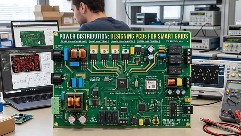
Key Principles in Designing PCBs for Smart Grids
Designing PCBs for smart grid operations requires a relentless focus on efficiency, safety, and reliability. The specific requirements for power distribution PCBs include:
Optimizing Trace Width and Copper Thickness
- The use of wide and thick copper foil traces can effectively reduce voltage drop, enhance current-carrying capacity and improve power transmission efficiency – this design is particularly crucial in high-power and high-frequency PCBS such as substations and electric vehicle charging piles.
Advanced Material Selection
- The selection of High glass transition temperature (high-TG) and flame-retardant (UL 94 V-0) PCB substrate can ensure the maintenance of operational stability under abnormal working conditions such as power surges and environmental stress.
- In solar and wind energy converters, metal core PCBS (MCPCBS) are adopted to achieve outstanding thermal management capabilities.
Thermal Management and Multilayer PCB Structures
- By adopting a multi-layer board structure with a dedicated power layer and a complete ground plane, the thermal conduction efficiency and impedance characteristics of the power distribution network (PDN) can be significantly enhanced, while effectively suppressing the common-mode radiation and edge radiation of electromagnetic interference (EMI).
- By arranging an array of thermal vias filled with heat conduction or electroplating, and combining the zoned isolation layout of heat sources and temperature-sensitive devices, heat can be quickly conducted to the heat dissipation layer or external heat sink, thereby ensuring the long-term thermal and reliability of the entire system.
Signal Integrity and EMI Shielding
- Rigorous PCB layout and routing can reduce crosstalk and ensure robust signal transmission – which is particularly crucial for cross-component that requires ultra-reliable data exchange in smart grid communication.
Redundancy and Scalability
- Modular and scalable PCB components enable the power grid to flexibly adapt to the growth of network scale, the integration of new technologies, and the impact of peak electricity consumption. By adopting redundant paths and hot-swappable modules, engineers can quickly replace or expand smart grid equipment without interrupting system operation.
- The built-in redundant design effectively enhances the system’s online rate, ensuring that the power grid can still provide flexible and reliable power supply services when faults occur or when new distributed energy sources such as solar and wind power are added.
Design Strategies for PCB Assemblies in Smart Grid PCB Production
| Strategy | Benefit | Relevant Tech/Term |
| Wide Copper Traces | High current support, less voltage drop | Power distribution, PCB material |
| Multi-Layer Board Structure | EMI reduction, compactness | Multilayer PCB, advanced PCB |
| Segmented Power/Ground Planes | Improved power integrity, lower noise | PCB assemblies, system stability |
| Modular, Redundant Layouts | Fault tolerance, scalability | Efficient smart grid, reliability |
| On-board Communication Modules | Real-time, resilient data transmission | Smart grid communication, digital technology |
Smart Grid Communication and Advanced PCB Material
Why Smart Grid Communication Matters
Smart grid communication is the core enabling technology for achieving truly efficient operation of the power grid. By enabling all devices within the power grid to share their operational status in real time, collaboratively execute demand response strategies, and possess fault prediction and rapid response capabilities, power outage events can be minimized to the greatest extent, and the integrity of the overall power grid can be enhanced.
- Communication between power grid components: It has gone beyond the scope of traditional SCADA systems. Currently, highly integrated PCB components can directly support multiple communication standards such as Wi-Fi, Zigbee, NB-IoT, cellular networks (4G/5G), and even satellite communication, achieving wide coverage and low latency data interaction.
- Power grid communication technology: It provides the physical layer and link layer foundation for real-time control, especially playing a decisive role in the smooth grid connection and energy dispatching of renewable energy sources with strong volatility and high uncertainty, such as photovoltaic and wind power.
Selecting PCB Material for Reliability and Performance
PCB material selection sets the foundation for all smart grid PCB solutions:
- FR-4 is the conventional default choice. However, for harsh smart grid environments such as outdoor substations and inverter stations, it is preferred to use laminates or Polyimide substrates with High glass transition temperature (high-Tg, usually >170°C) and Low dielectric loss (Low Df, such as ≤005) To ensure electrical stability and mechanical strength under high temperature and high humidity conditions.
- For high-frequency PCB application scenarios such as radio frequency monitoring and real-time communication, dedicated materials with strictly controlled dielectric constants (Dk) and high frequency stability (such as Rogers, Taconic, etc.) should be adopted to minimize signal transmission loss and phase distortion and ensure the quality of communication links.
- Metal core PCBS (MCPCBS, such as aluminum-based and copper-based boards) are ideal choices for power management circuits in solar and wind energy inverters. Their high thermal conductivity (typically >1.5 W/mK, and up to >3 W/m·K for copper-based ones) can quickly dissipate the heat of power devices, significantly enhancing the long-term reliability of the system.
Challenges in Smart Grid PCB: Reliability and Solutions for Smart Grid Operations

Key Challenges in Smart Grid PCB Assemblies
Environmental Stressors
- Extreme temperature cycles, long-term ultraviolet (UV) radiation, and high relative humidity and other harsh operating conditions can significantly deteriorate the PCB components in outdoor smart grid infrastructure, which may lead to medium breakdown, electrochemical corrosion, and even complete system failure. Countermeasures: Choose to use conformal coating/sealed housing/UV-resistant PCB substrate.
Maintaining System Stability
- Complex smart grid systems experience unpredictable loads. Designers need advanced simulation and stress-testing to confirm that all PCB assemblies withstand both routine and extraordinary power flows—this is crucial to avoid outages.
Communication Integrity
- In a PCB layout where power electronic circuits and high-frequency signals coexist, achieving interference-free data transmission is highly challenging. Only by adopting rigorous PCB layout and routing, as well as zonal shielding and electrical isolation strategies (such as ground line division, common-mode chokes, optocoupler or magnetic coupler isolation) can reliable physical layer guarantees be provided for the optimized smart grid communication.
Lifecycle and Scalability
- With the rapid absorption of new technologies by the smart grid, PCB components must have forward compatibility capabilities. Adopting a plug-and-play modular design, functional upgrades can be achieved without replacing the entire system, thereby reducing electronic waste and maintaining the efficiency and sustainability of the smart grid operation.
Solutions for Smart Grid PCB and Optimized PCB Production
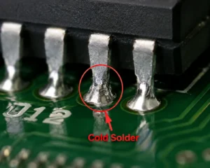
- For critical power circuits carrying high currents, the adoption of Through-Hole Technology (THT) can significantly enhance the mechanical strength of solder joints and their resistance to thermal cycling fatigue compared to the sole use of surface mount technology (SMT), ensuring long-term operational reliability.
- During the PCB design stage, simulation tools should be introduced to jointly model the interaction between power flow distribution and electromagnetic fields, achieving prediction and optimization of voltage sags, current density, crosstalk and electromagnetic interference (EMI), thereby reducing the cost of prototype iteration and shortening the development cycle.
- The adoption of low-volatile organic compound (Low-VOC) processes, recyclable substrates, and lead-free materials that comply with the RoHS Directive not only helps to build a sustainable and efficient smart grid operation system but also meets increasingly strict environmental protection regulations.
PCB Assemblies and Advanced Manufacturing Technologies
The Role of Modern Manufacturing in Efficient Smart Grids
Today’s PCB production for smart grid applications involves advanced automation and precise quality control:
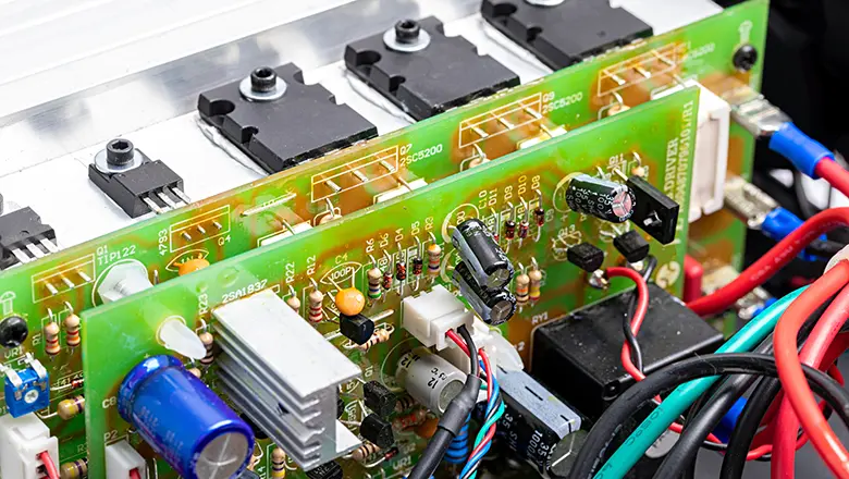
- Surface Mount Technology (SMT) and through-hole technology for robust, high-power assemblies.
- Automated Optical Inspection (AOI) and X-ray testing for efficient defect detection in multilayer and complex boards.
- CNC and laser drilling for consistently sized vias (critical for multilayer PCB reliability).
High-Frequency PCB Solutions for Smart Grid Technologies
With the continuous evolution ofsmart grid technology, PCBS must simultaneously support the increasingly high operating frequencies on both the power conversion side and the wireless communication side: the former includes high-frequency harmonics generated by fast-switching devices such as IGBTs and SiC MOSFETs, while the latter covers the high-frequency frequency bands used by various wireless communication protocols.
- For high-frequency signals, Microstrip or Stripline structures should be adopted for wiring, and in the PCB layout, the analog/power circuits should be strictly physically separated from the digital communication lines to reduce crosstalk and common-mode interference.
- For the signal transmission lines in the smart grid communication module, substrate materials with controlled impedance (such as 50Ω, 75Ω or 100Ω differential) and Low dielectric loss (Low Df) should be selected to ensure the integrity and transmission quality of high-frequency signals.
PCB Solutions, High-frequency PCB, and the Future of Smart Grids
Next-Generation PCB Solutions for Efficient Smart Grids
- The integration of multi-layer PCBS and intelligent sensing: The multi-layer of PCBSdesign that integrate embedded sensors and wireless connection capabilities has become the core foundation for building a future-oriented smart grid operation system.
- Embedded AI and edge computing: PCBS equipped with board-level microcontrollers (MCUS) or lightweight AI acceleration units can achieve local analysis of power quality parameters and prediction of equipment maintenance requirements, thereby reducing power outages and enhancing the intelligence level of power grid operation.
- Blockchain integrated application: In the PCB design of smart grids, hardware security modules (HSM) or trusted execution environments (TEE) that support blockchain technology can be built in for device identity authentication and data traceability, especially having significant application prospects in the distributed energy trading market.
The Future of Smart Grids: Advanced PCB Technology
- The development direction of self-healing power grids: Advanced PCB components with local decision-making capabilities, which can automatically reconfigure power paths when faults or power outages are detected, promoting the evolution of power grids towards self-healing architectures.
- Interconnected microgrid: An interconnected microgrid composed of multiple small grid units can actively switch to island operation mode when the main grid fails and continuously supply power relying on renewable energy – the realization of this capability is highly dependent on robust PCB components and modular control units.
New Technologies Embedded in Smart Grid PCBs
| Technology | PCB Impact | Grid Benefit |
| Wireless IoT Modules | Real-time monitoring, demand response | Faster outage detection, granular management |
| Powerline Communication | Data over high-voltage power lines | Simplifies retrofits, stable communication |
| Embedded AI/ML | Predictive control, adaptive optimization | Energy efficiency, preventative maintenance |
| Blockchain Chips | Secure authentication, data traceability | Greater security, trustworthy transactions |
| High-Frequency Routing | Stable communications, better signal | Reliable SCADA, AMI, grid automation |
Optimize and Future-Proof: Extended Tips for Efficient Smart Grid PCB Production

- Engage PCB partners with real-world smart grid experience: True professional ability is not only reflected in theoretical design, but also in on-site verification and experience accumulation of board selection, layout and wiring, and electrical performance under the actual working conditions of the power grid – partners with on-site deployment cases such as substations and inverter stations should be given priority.
- Plan for modular upgrades and expansions: By adopting slot-type connectors, pin headers or standardized board card sizes (such as COM Express, SOM, etc.), it ensures that the power grid can quickly integrate emerging technologies without replacing the entire system, achieving forward compatibility and flexible expansion.
- Map all communication paths: In the design, a detailed communication path diagram between power grid components (including optical fibers, radio frequency, cellular networks or power line carriers, etc.) should be drawn. Based on this, the PCB layout should be optimized to minimize the coexistence interference between different signals and maximize the system’s online rate.
- Prioritize sustainability in PCB material choices: Select recyclable or biodegradable substrates (such as bio-based FR-4), water-based fluxes and lead-free solders to meet environmental protection standards such as RoHS and halogen-free, and build future-oriented green smart grid PCB components.
- Embrace digital twins and simulation: Build a digital twin model covering the entire smart grid system during the design phase, and conduct pre-simulation verification on power flow distribution, electromagnetic interference (EMI), and communication link quality – even before the first prototype board is manufactured.
Conclusion: Powering the Future with Smart Grid PCB Solutions
The evolution from traditional power grids tosmart grids is profoundly reshaping the way energy is utilized in households, businesses and public utilities. As the core driver of this transformation, LHD TECH’s PCBs in smart grid systems solution plays the triple roles of “intelligent hub”, “nerve endings” and “structural backbone” – not only supporting the physical architecture of modern power distribution, but also from the seamless integration of renewable energy sources like solar and wind power to highly reliable real-time communication Then comes the elastic operation of the power grid with self-healing capabilities for faults.
To keep pace with this revolution:
- Choose PCB material and PCB assemblies with field durability, high current handling, and flexibility for upgrades.
- Integrate communication technologies natively—SCADA, Powerline Communication, IoT—and optimize every board for signal integrity and power efficiency.
- Leverage modular, advanced PCB solutions for scalability, sustainability, and speed—ensuring your energy grid can accommodate the demands and technologies of tomorrow.
As smart grid technologies and PCB technologies co-evolve, operators, utility engineers, and innovators will only succeed if they treat PCB design and manufacturing as strategic imperatives. The grids that deliver greater control over energy consumption, maximize uptime, and empower the clean energy transition will be those with the smartest, most adaptable PCB assemblies at their core.
Partner with experts in PCB production and smart grid solutions who understand the unique challenges of modern energy distribution, power efficiency, and real-time communication requirements. Embrace a future where your power grid is not just robust but also intelligent—capable of leveraging new technologies, responding to dynamic power consumption trends, and integrating seamlessly with renewable energy sources like solar and wind.
Key Takeaways for Smart Grid Success with Advanced PCBs
- Strategic PCB Design is Mission Critical: Every device on the smart grid, from advanced metering systems to inverter modules, relies on the integrity and intelligence of its PCB assemblies to optimize performance, prevent energy loss, and ensure smooth power flow across the grid.
- Modern PCB Solutions Enable Real-Time Control: Embedding communication modules, edge computing, and security chips in your PCBs provides a foundation for robust smart grid communication and system stability.
- Material Selection Drives Reliability: Choosing the right PCB material—from high-Tg laminates to metal-cores and high-frequency PCB substrates—can make or break your smart grid components’ longevity and thermal performance.
- Modular Designs Future-Proof the Grid: Designing for upgrades through modular, multilayer PCB approaches ensures your network remains scalable, adaptable, and ready for tomorrow’s energy challenges.
- Eco-Conscious Manufacturing Matters: As the world demands greener power, build sustainability into your PCB manufacturing—think recycled substrates, lead-free solders, and energy-efficient assembly.
Frequently Asked Questions (FAQs) about PCBs and Smart Grids
Q1: How do PCBs in smart grids differ from traditional PCB assemblies?
A: PCBs for smart grid applications must handle higher power, endure harsh environments, and integrate complex communication modules to enable real-time monitoring, greater control over energy consumption, and instant grid response—far beyond the needs of typical consumer or industrial PCBs.
Q2: What is the role of high-frequency PCBs in the smart grid system?
A: High-frequency PCBs ensure stable, reliable smart grid communication, particularly in wireless modules, real-time sensors, and PLC-backed data transmission. This is key for dynamic energy balancing and outage management.
Q3: How can PCB design help prevent power outages on the grid?
A: By implementing redundant circuits, advanced thermal management, EMI shielding, and real-time monitoring, PCBs can quickly detect load spikes or faults, trigger automated switching, and support the restoration of service—all crucial to minimize outages.
Q4: What are key considerations for optimizing PCB production for smart grid solutions?
A: Focus on selecting proper PCB material, robust multilayer structures, modular and scalable layouts, eco-friendly fabrication processes, and comprehensive testing (thermal cycling, EMI, power cycling) to ensure reliability and future expansion.