Introduction to Wave Soldering
Wave soldering is one of the core processes for us to provide high-reliability electronic manufacturing services. As mass soldering technology that has been verified for decades, it is primarily used for through-hole components and can also perfectly support the production of circuit boards with soldering through-hole components. In simple terms, wave soldering is a process where the solder electronic components onto printed circuit boards (PCBs) passes through the molten solder wave at a constant speed through a conveying system, thereby achieving synchronous connection of all pins and pads. This automated batch soldering method is incomparable to manual soldering with soldering irons in terms of consistency, production efficiency, and mechanical strength of solder joints.
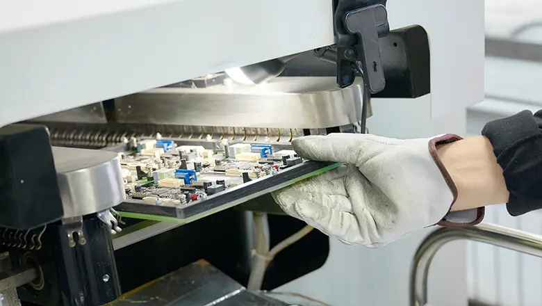
In actual used to solder surface mount technology (SMT) parts, we will fix the PCB with components inserted onto the conveyor chain. After flux spraying and preheating, the board surface will pass over the continuously surging solder peaks at a specific Angle. The design of this dynamic wave peak is crucial – it not only ensures that each pin and plated through hole is fully wetted to form a reliable metallurgical bond, but also effectively avoids the bridging and shadow effects that are prone to occur in traditional dip soldering. For this reason, in the process workshop of LHD TECH, wave soldering remains the main equipment for handling heavy components such as high-current connectors and transformers. These products are ultimately used in automotive electronics, industrial controllers and power modules, and have extremely high requirements for the fatigue strength and shock resistance of the solder joints.
Understanding the differences between wave soldering and reflow soldering process is very helpful for us to optimize the production plan. When the customer’s design mainly consists of through-hole components or has large-sized irregular components, we will give priority to recommending the principle of wave soldering solution. For surface mount designs with dense components and miniaturization, reflow soldering processes will be adopted. LHD TECH masters both of these core soldering technologies and can flexibly formulate the most suitable process flow based on the actual layout and reliability requirements of each PCB.
History and Principle of Wave Soldering

Origins of Wave Solder Soldering Processes
In the early years of making electronic products, all the component soldering on the circuit board was done by hand. The workstations are filled with soldering irons. The quality of the products is entirely dependent on the soldering skills of the engineers. It was not until the middle of the last century that wave soldering process as a whole improved the quality of PCBA. Moreover, it has achieved an automated and repeatable batch production process, enhancing the efficiency and quality of the entire industry.
- Dip soldering involves immersing the board with the components inserted into a molten tin furnace, while drag soldering involves dragging the board along the surface of the solder. Although these two methods initially achieved batch welding, their process control capabilities were limited – they were prone to oxidation, unstable wetting effects, and problems such as bridging, solder spikes, and voids were likely to occur, and their production capacity was difficult to meet the rapidly growing demands of the electronics manufacturing industry at that time.
- The core principle of wave soldering is: through a pump and a flow guide structure, the liquid solder in the solder bath is continuously sprayed out from a narrow nozzle, forming a stable flow with a certain wave height “wave peak”. The dynamic solder wave peak constantly updates the surface, the oxide is carried away, and the wetting force of the solder is always in the best state. During actual production, the PCB with components inserted is driven by a conveyor chain and smoothly passes over this wave peak at a specific Angle and speed. At the same moment, all the pins and pads of the components are fully submerged in hot solder, completing a reliable metallurgical connection.
The Principle of Wave Soldering
Although the principle of wave soldering is simple, its process logic is highly efficient. A PCB with completed plug-in assembly first passes through a preheating zone to raise the surface temperature, and then its bottom surface passes through a continuously surging peak of molten solder wave at a specific Angle and speed. Under the combined action of surface tension and wetting force, the solder rapidly wets the exposed metal surface and simultaneously fills the through-holes upwards, forming a full and reliable solder joint.
Flux plays a crucial role in this process. It is applied to the PCB in advance during the preheating stage. One reason is to remove the oxide on the surface of the pins and pads, and the other is to reduce the surface tension of the molten solder, thereby enhancing the wettability. Ensure that the solder can fully spread and penetrate during welding, and ultimately form a stable and reliable metallurgical bond.
Key steps:
- PCB preparation and component placement.
- Flux is applied to the underside of the board.
- The board passes over a wave of molten solder.
- Excess solder is removed as the board exits, often with air knives or mechanical fixtures.
This process used is primarily used for through-hole technology, though deft engineering can adapt it for certain types of surface mount components.
Key Equipment in the Wave Soldering Process
Wave Solder Machine
On the wave soldering production line in the LHD TECH workshop, the wave soldering machine is the core equipment of the entire process system. The tin bath we have configured can hold tens of kilograms of solder. It fully adopts lead-free tin-silver-copper (SAC) alloy that complies with RoHS standards. The solder temperature is stably controlled within the process window through a precise temperature control system – for lead-free processes, it is usually set between 245°C and 260°C. Inside the tin bath, the molten solder is continuously pumped out from the peak nozzle by a motor or electromagnetic pump, forming a stable and controllable standing peak. Based on different board types and component layouts, we precisely adjust the peak height, waveform shape and transmission Angle to ensure that every PCB passing through achieves the best soldering effect.
Fluxing System
Before the soldering process, flux is a chemical compound applied to the PCB’s underside via a foaming or spray system. It cleans oxide layers, enhances wetting of the solder, and prevents solder balls and bridging during passage through the wave.
Preheating System
The preheating stage is a crucial step in the wave soldering process that determines the welding quality. Before the PCB enters the solder wave peak, it will pass through a gradually heated preheating zone. This stage first effectively reduces the temperature difference between the board surface and the high-temperature solder through gradient heating, avoiding damage to components due to thermal shock. Secondly, preheating activates the pre-coated flux, bringing it into the optimal activation window to fully exert its chemical effect in removing oxides. Meanwhile, the solvent components in the flux fully volatilize during the preheating stage, preventing the residual solvent from instantly vaporizing during soldering, which could lead to defects such as spatter, voids or solder balls.
Conveyor and PCB Positioning
The conveyor system is designed to ensure that the board moves steadily and accurately. To ensure that the PCB moves smoothly at the set Angle and speed from entry to exit, the bottom of the board is always directly facing the solder wave peak. If there is jitter, lag or the speed fluctuates between fast and slow during the transmission process – it will cause some solder joints to be insufficiently wetted, resulting in solder sticking and sharp points. Therefore, on our production line, the calibration of the conveying system is the foundation of process control. Whether it is stable and accurate directly determines the consistency of batch welding.
Cooling and Inspection
After passing the peak, enter the cooling zone – the solder joint should not cool down too quickly. After it solidifies gradually, the thermal stress generated during the welding process is released to prevent microcracks or brittle fractures inside the solder joint due to a large temperature difference between hot and cold. After welding is completed, manual visual inspection and AOI automatic optical Inspection systems are combined. AOI relies on the high-speed scanning of the visual system to automatically compare the shape of the weld points, which is more efficient and stable.
How the Wave Soldering Process Works (Step-by-Step)

The wave soldering process can be broken down into the following detailed actions, each essential to form reliable solder joints and robust PCB assembly:
1. Solder and PCB Preparation
- Components are placed on the PCB.
- The board is cleaned, especially on the underside of the board, to remove contaminant films or oxide.
- Solder pot is filled with the chosen solder alloy, verifying the right solder temperature and composition.
2. Flux Application
- Flux is applied to the PCB by spray or foam. This dissolves oxides and ensures the solder wets well as the board is passed over the molten wave.
3. Preheating the PCB
- Before the board enters the wave peak, the PCB is heated first: to evaporate the solvent components in the flux first. Then release the activity of the flux; Finally, let the overall temperature of the board rise gradually.
- The key to the temperature curve is to ensure that the temperature distribution across the entire board is uniform. Be cautious of thick boards as they absorb more heat and dissipate it slowly. If there are pieces on both sides, the heat capacity will be uneven, the temperature will be insufficient, and the wetting effect of the solder will be poor. In practical operation, every time we change the plate type, we will measure it once with a temperature measuring plate to adjust the temperature of each section of the preheating zone and the each section to an appropriate degree.
4. The Solder Wave
- The board is passed bottom-first over a standing molten solder wave.
- The liquid solder covers every exposed joint—this masks soldering through-hole components, fills holes in the PCB, and forms solder cones (“volcanoes”) at the pin exits on top.
5. Solder Separation and Excess Removal
- As the printed circuit board (PCB) moves away from the wave crest, the excess solder flows back under the force of gravity. Sometimes, devices such as air knives or vibration fixtures are also used to assist in the reflow process.
- The control of the separation speed is of vital importance and helps prevent the formation of defects such as sharp solder whiskers, solder balls or Bridges.
6. Cooling and Inspection
- The main purpose of controlled cooling step is to prevent the solder from developing cracks or thermal stress during solidification.
- During the inspection, the main focus is on whether the solder filling is in place and whether there are any issues such as bridging, solder balls or cold soldering.
7. Flux Removal (if needed)
- To thoroughly remove residual ions from key products, the flux must be cleaned first to ensure long-term reliability.
Critical Factors for Solder Quality in PCB Assembly
Several critical variables must be monitored and tuned for repeatable, robust solder joints:
- Solder temperature and pot composition: Always maintain at desired temperature to properly melt the solder and connect all joints.
- Preheat profile: Step the temperature to avoid warping or damaging sensitive parts.
- Wave height and conveyor speed: Set precise contact time—too much leads to bridging, too little causes skips.
- Component orientation: Arrange components to minimize shadowing and maximize wave contact. Place taller components downwave, away from the wave’s entry.
- Pad and hole dimensions: Proper sizing ensures the correct amount of liquid solder fills each joint.
- Flux type and delivery: Adequate, even coverage for clean wetting, without causing excess residue or shorts.
PCB Design for an Effective Wave Soldering Process

Wave soldering is deeply influenced by PCB design:
- Pad and hole design: Ensure that the through-hole function is in place and the filling is full. When designing the pads and vias, the dimensions of the annular pads and hole diameters must strictly comply with the IPC standards.
- Component spacing: There should be sufficient spacing between components and pins to avoid bridging.
- Wave direction: Align connectors and dense components parallel to the solder wave for more even wetting of the solder.
- Solder mask: When solder mask is applied, a solder mask bridge should be added between the pins to prevent bridging between fine-pitch pins. If it is a complex layout, remember to clearly define the soldering area for the solder mask layer. This way, the soldering during wave soldering will be more uniform and the accumulation of excess solder can also be reduced.
- Thermal reliefs: If hot pads are needed for connecting large copper surfaces, it is recommended to use a heat relief design to prevent the pads from heating up quickly, ensuring that the solder melts fully and the solder joints are more reliable.
- PCB thickness: Optimize thickness to prevent sagging as the PCB moves through the hot solder—thin boards may sag and create inconsistent solder connections, especially when the solder wave height is high.
- Component orientation: Critical for double-sided PCB assemblies or when soldering surface mount components. Place sensitive or large components away from the wave entry side to avoid shadowing, and ensure that tall or heat-sensitive components won’t prevent the wave from properly contacting every joint.
Applications: Where and Why Wave Soldering Is Used
The wave soldering process is mainly used to solder electronic components onto printed circuit boards when durability, speed, and throughput are essential. It’s especially favored in:
- Mass soldering for automotive electronics: The batch soldering of automotive electronics requires durable connectors, relay bases, and highly reliable interfaces, which are basically accomplished by wave soldering.
- Industrial equipment and power supplies: For industrial equipment and power supply products, circuit boards need to handle relatively large currents, plug-in components are large in size, or mechanical strength requirements are high. The solder joints formed by wave soldering have good consistency and can meet the performance requirements of the products.
- Consumer electronics: In consumer electronics, such as home appliance control boards, LED light strips, and audio power amplifiers, there are both connectors and surface mount components on them, which belong to mixed assembly processes. A reliable and automated method is needed for soldering, and wave soldering is very suitable.
- Medical equipment and aerospace: In the fields of medical equipment and aerospace, the quality inspection and reliability requirements for solder joints are extremely strict. Automated processes like wave soldering can provide complete traceability and process records, so they are generally preferred for such applications.
Advantages and Disadvantages of the Wave Soldering Process
Advantages
- Efficiency: Wave soldering can complete the welding of hundreds of solder joints simultaneously at one time. In mass production, it is the fastest way to solder components on circuit boards.
- Consistency: Automated operation avoids the influence of human factors. As long as the equipment parameters are adjusted properly, the temperature, wetting and filling effect of each solder joint can all reach the ideal state.
- Great for Through-hole Soldering: If the board mainly consists of plug-in components, power devices or connectors, wave soldering is the most suitable choice.
- Lead-free Compatibility: The current wave soldering equipment and process control can handle both lead-free solder and traditional lead-based solder, fully meeting the current environmental protection requirements.
- Scalability: A wave soldering line can be quickly switched to produce different products by changing the fixture and adjusting the program. This flexibility is very practical for contract manufacturers.
Disadvantages
- Limited SMD Handling: If there are many close-fitting surface mount components on the board, wave soldering may also be hindered, and selective soldering should be used to make up for it.
- Design Constraints: When laying out the PCB, channels should be reserved for wave crests. If the board density is too high or 3D stacking is done, it is convenient to use the wave soldering process.
- Thermal Stress: Some sensitive components, if placed on the bottom of the board and in direct contact with high-temperature solder, cannot withstand thermal shock.
- Maintenance Needs: The scum and oxides in the tin pot should be removed regularly to prevent flux blockage, and the temperature control should also be calibrated at any time.
- Flux Residues: The residual flux still needs to be specially washed after soldering, especially for those products with high requirements for safety and reliability.
Wave Soldering vs. Reflow Soldering
Both the wave soldering process and the reflow soldering process are essential in today’s PCB assembly toolkit, but they serve different purposes.
Wave Soldering:
- Best used to solder through-hole components and mass connections.
- Uses a wave of solder (hot, melted solder) to form solder joints on the bottom of the PCB during the passage through the wave.
- The automated equipment tints all the exposed metal on the bottom surface of the board at one time.
- Suitable for large-sized components, connectors, and designs with high mechanical strength requirements.
Reflow Soldering:
- It is mainly used for soldering surface mount components, such as surface mount resistors, capacitors, ics, etc., and they are placed on solder pads coated with solder paste.
- During soldering, the solder paste is melted by controlling the convection of hot air or infrared heating (that is, the “reflow oven”) to form the solder joints.
- Allows exact control over soldering surface mount pads and minimizes thermal stress.
Comparison Table:
| Characteristic | Wave Soldering Process | Reflow Soldering Process |
| Used for | Through-hole; some SMDs | Surface mount components |
| Solder application | Molten solder wave | Solder paste |
| Process temperature | 245–260°C | 220–250°C |
| Process used | Board is passed over a wave | Board is heated in reflow oven |
| Component location | Bottom of the board | Either or both sides |
| Design constraints | Requires pad/hole and orientation | Pad design for each device |
| Automation | High | High |
When to Use Each: Wave soldering is a commonly used and economical choice for the mass production of through-hole plates, especially in situations where the reliability requirements for connectors or power components are relatively high. Reflow soldering is better at dealing with high-density, complex surface mount boards, or circuit boards with components attached on both sides.
Wave Soldering for Surface Mount Components
Although wave soldering is mainly used for soldering through-hole components, if the design is adjusted, it can also be used to complete some component surface mount. This operation method can reduce costs and improve practicality.
Techniques for Soldering Surface Mount Components:
- Glue and Wave: First, apply glue to the bottom surface of the board, fix the surface mount components, and then go through wave soldering. It is commonly found in MELF, SOIC, or large-sized passive components.
- Selective Soldering Pallets: Shield SMDs and expose only desired pins and pads to the solder wave—used for complex hybrids.
- Optimized Pad and Layout: For surface mount components that must undergo wave soldering, the spacing and size of the pads need to be appropriately increased, and the placement direction of the components should also avoid the wave entry as much as possible to reduce the shadow effect.
Common Defects and Troubleshooting in the Wave Soldering Process
Understanding and troubleshooting soldering defects is key to effective mass soldering and robust PCB assembly.
Common Defects:
- Solder Bridges: Prevent solder connection between pins, such as applying too much solder, having pins too densely packed, or using incorrect parameters for wave soldering.
- Cold Solder Joints: If the solder joints appear dull or rough, it is usually due to insufficient temperature, poor wetting, or rapid cooling.
- Solder Balls: If round solder beads stick to the board, it is often caused by flux splashing or poor solder reflow.
- Non-fill or Skipped Joints: The solder in the hole is not filled up or not soldered, which is usually related to the speed of passing through the board, the application of flux, or the inappropriate size of the pad/hole diameter.
- Icicles and Dross: The appearance of solder burrs on the solder joints or excessive surface oxidation residues is mainly caused by incorrect solder temperature, too slow separation speed, or failure to clean the solder pot in time.
Troubleshooting Tips:
- Inspect flux application: Too little or blocked spray can cause non-wetting.
- Calibrate preheater: Uneven heating creates stressed, unreliable joints.
- Tune conveyor and wave height: Adjust speeds to allow proper excess solder removal.
- Clean and refresh the solder pot: Accumulated oxide (dross) impacts solderability and pot life.
Typical Defect Causes and Solutions
| Defect | Likely Cause | Remedy |
| Bridges | Excess solder/wave height high | Lower wave, increase pad spacing |
| Cold joints | Low temp or rapid withdrawal | Boost preheat, slow conveyor |
| Solder balls | Excess flux or rapid heating | Adjust preheat, review flux choice |
| Skipped joints | Insufficient flux or poor pad design | Improve fluxing, review pad/hole layout |
Safety and Environmental Considerations in Mass Soldering
Worker Safety
- Molten solder is hazardous: Temperatures often exceed 250°C—strict protocols required to prevent burns or fire.
- Lead and chemical exposure: RoHS-compliant lines are typically lead-free, but even modern solder alloys contain metals needing careful handling. Proper PPE and fume extraction systems are essential.
- Regular training: Staff must be trained in equipment operation, emergency response, and safe chemical handling.
Environmental Issues
- Proper dross disposal: Solder dross must be disposed of as hazardous waste or recycled by certified vendors never discard oxide or spent solder in regular trash. This protects both factory personnel and the broader environment.
- Switch to lead-free solder: Most modern wave soldering machines and PCB assembly lines now use lead-free solder alloys (like SAC305), dramatically reducing hazardous waste and aligning with global RoHS directives. Maintain strict separation of leaded and lead-free processes to avoid contamination.
- Waste water from flux removal: When water-soluble fluxes are used and boards need to be cleaned after soldering, rinse water containing flux residues must be treated according to local regulations before disposal.
- Energy management: Wave soldering machines continuously keep solder at a high temperature, consuming electricity. Implement programmable heat management and only run machines at idle or desired temperature when production requires to save energy.
Trends and the Future of Wave Soldering
Wave soldering remains a crucial process in electronics manufacturing, but it continues to adapt:
- IoT-Driven Process Monitoring: Modern wave soldering machines are often equipped with sensors and cloud connectivity, enabling real-time tracking of solder temperature, wave height, flux use, and conveyor status.
- Selective Soldering Technologies: As PCB design becomes more complex, selective soldering allows precise, programmable solder application to just the parts of the board that need it—even with components on both sides of the PCB.
- Automated Quality Control: AI-powered automated optical inspection (AOI) systems now check every joint post-soldering, rapidly identifying defects and feeding feedback into the soldering processes for continuous improvement.
- Advanced Alloys and Chemistries: The search for ever more reliable, oxidation-resistant, and environmentally benign solder materials leads to new mixtures of tin, silver, copper, and additives—forming best-in-class solder connections for critical industries.
- Green Manufacturing: Sustainability goals drive improvements in energy efficiency, dross recycling, and the selection of less-toxic fluxes and solder masks, making wave soldering not just effective, but also eco-friendly.
- Digital Twins and Simulation: New digital manufacturing platforms simulate soldering through-hole and surface mount processes, allowing DFM engineers to predict solder joint quality and optimize designs before the first board is built.
Frequently Asked Questions: The Wave Soldering Process
What types of solder are used in the wave soldering process?
Most modern lines use lead-free alloys such as SAC305 (Tin-Silver-Copper), supporting RoHS compliance. Historically, tin-lead alloys (Sn63Pb37) were common but are now restricted for most products.
Can wave soldering be used for boards with components on both sides?
Yes, by careful sequencing. Typically, surface mount technology parts are reflow-soldered first (top side or sometimes both sides of the PCB), then the through-hole side of the board is wave soldered. Sensitive bottom-side SMDs must be adhesive-fixed and compatible with the solder temperature.
How do you optimize the wave soldering process for minimum defects?
- Profile the preheat and solder wave temperature
- Use proper flux type and amount for oxide removal and wetting
- Monitor pad and hole sizing, adjust conveyor speed, and ensure all solder is drained as the PCB moves away from the wave
- Frequently inspect for solder balls, bridges, and skipped joints using AOI
Why is proper PCB design so important for the wave soldering process?
PCB design influences every aspect of mass soldering: from how the wave reaches the pad, to the form solder joints take, to prevention of solder bridges and ease of inspection. Poor PCB design can thwart even the best-tuned wave solder process.
How does wave soldering compare to reflow soldering in terms of reliability?
For through-hole connectors or high-power components, wave soldering offers superior mechanical strength and lower contact resistance. For high-density, fine-pitch SMDs, reflow soldering provides better control and precision.
What maintenance is required for wave solder machines?
Regular dross removal, pot cleaning, pump and wave nozzle checks, thermocouple calibration, and flux system cleaning. Neglecting these can cause increased solder defects and decreased machine life.
Conclusion: Is Wave Soldering Right for Your PCB Assembly?
Wave soldering is a technique that continues to underpin the most demanding, high-reliability sectors of electronics manufacturing—even as reflow soldering and SMT dominate miniaturized consumer devices. If your application calls for robust solder connections, large connectors, or the need to solder electronic components onto printed circuit boards quickly and at scale, wave solder is often the best way to solder.
Choosing between wave solder and reflow soldering is not only about the components you use, but also your PCB design, the production volumes you anticipate, and the level of mechanical stress your assemblies will experience.
To maximize your success:
- Apply DFM to every board; tune your soldering processes from the start.
- Collaborate with manufacturing partners early for hybrid board strategies.
- Invest in regular process audits and equipment maintenance for consistent, high-yield assembly.
The wave soldering process is proven, adaptable, and, with continued innovation in equipment and process control, is set to remain a cornerstone of PCB assembly and best-in-class soldering processes for years to come.
Have a complex or cutting-edge wave soldering challenge?
Consult with experienced partners, reference IPC standards, and never underestimate the role of design and process planning. The right soldering process can be the difference between a product that just works—and one that excels for years in the field.