Introduction: Why PCB Testing Methods Matter
At LHD TECH, we understand that printed circuit boards (PCBs) are the foundation of all modern electronic devices. Whether a product is a reliable and stable tool or a potential source of frequent field failures often hinges on the rigor of its testing and inspection processes. Each PCB testing method can reveal different types of defects—from hidden solder bridging, missing components, and misaligned integrated circuits to microcracks invisible to the naked eye. With LHD TECH’s tailored test method, this complete guide to PCB quality ensures your products not only function perfectly in initial verification but also operate reliably and reliably in real-world environments.
Modern electronic products are facing increasing pressure: shorter prototype iteration cycles, ever-increasing circuit complexity, and increasingly stringent consumer reliability demands. LHD TECH’s efficient guide to PCB testing methods help you verify that every circuit board meets predetermined design standards and ensure that every board leaves the factory with zero defects. This article serves as your ultimate guide to PCB testing methods, breaking down each key step and tool required to ensure reliability, verify assembly quality, confirm circuit functionality, and meet the most stringent IPC standards.
PCB Manufacturing and the Need for Thorough Testing
Why Testing and Inspection Are Non-Negotiable in PCB Assembly
Successful pcb manufacturing doesn’t end with assembling hundreds of electronic components on a board. As PCB trace density and chip packaging integration continue to rise, thorough testing has become a core pillar for the successful delivery of every project. Failure to deploy appropriate testing methods at the right stage can result in catastrophic field failures, severe damage to brand reputation, and even compliance risks. For example, a simple solder bridging that is difficult to detect by manual visual inspection is enough to cause the entire module to fail; while system-level problems such as electrical leakage, surface contamination, and integrated circuit functional defects can also occur.
List: What Can Go Wrong Without Proper Inspection?
- Solder Voids and Bridges: Cause electrical short circuits, intermittent failures, and significantly reduce long-term reliability.
- Component Placement Errors & Missing Components: Directly lead to PCB malfunction and inability to operate normally.
- PCB Trace Damage: Causes signal attenuation, impedance mismatch, and even open circuit failures.
- Contamination and Flux Residue: Induce long-term electrochemical corrosion, creating potential field failure hazards.
- Thermo-Mechanical Stress: Causes cracks in traces and vias, especially prominent in multilayer, high-density interconnect (HDI) assemblies.
Understanding IPC Standards in PCB Manufacturing
Every test method for PCBs is framed by global norms established by IPC standards. These standards define the level of reliability, allow you to classify products by their use-case criticality, and guide inspection and testing protocols at every step.
Guide to PCB IPC Classifications
| IPC Class | Application | Reliability Level | Typical Test Coverage |
| 1 | Consumer Electronics | Basic | Visual, AOI, Sampling ICT |
| 2 | Office, Automotive, Industrial | Moderate Reliability | AOI, FCT, ICT, X-ray (as needed) |
| 3 | Aerospace, Medical Devices | High/Zero-defects | AOI, X-Ray, ICT, FCT, Burn-In, JTAG |
Key Point: For Class 3 (e.g., medical or military PCBs), full traceability is required for every assembled PCB, and often, 100% inspection and multiple type of testing are mandated.
Complete Guide to PCB Testing Methods
Thorough and efficient PCB assembly testing requires a combination of automated and manual methods designed for the type, volume, and reliability standards of your circuit board. Let’s break down the seven core pcb testing methods and expand with real-world tips, examples, and selection advice.
Bare Board Testing – The Basic Test for Circuit Boards
What Is Bare Board Testing?
Before any IC or resistor is soldered, basic testing is performed on the bare PCB with unassembled components. This verifies electrical continuity, checks PCB trace integrity, and confirms that each net is implemented as designed: no open circuits, no short circuits, and correct connections. This step is crucial for both mass production and prototyping.
What Does This Test Method Catch?
- Open circuits, shorted nets, misaligned drills.
- Faulty vias in multi-layer boards.
- Early process errors before expensive assembly.
Flying Probe Testing: Flexible Test Methods for Prototypes and Low-Volume PCBs
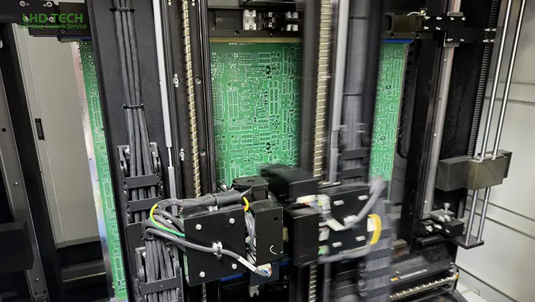
What Is Flying Probe?
Flying probe is a flexible, probe-based, non-fixture test method used for prototype and low-volume production. It adapts easily to changing designs since software, not hardware, sets test points. This makes it a go-to inspection step for New Product Introduction (NPI).
How It Works
- Automated robot arms deploy multiple probes to contact pads and vias.
- Verifies opens, shorts, correct value and orientation of individual components.
- No expensive test fixture needed—great for circuit boards that change frequently.
Example – Prototype Verification
A startup’s wearable sensor prototype underwent flying probe testing, revealing misaligned capacitors and a missing resistor—not seen by the earlier AOI sample. By catching these errors before ICT or full-volume assembly, rework costs and production delays were eliminated.
List: Key Benefits
- Fast setup for new circuit layouts.
- Ideal for design validation, component value checks, even for fine-pitch and mixed technology boards.
- Our program is very flexible, whether it’s for rapid prototyping and iteration or for multi-variety, small-batch production.
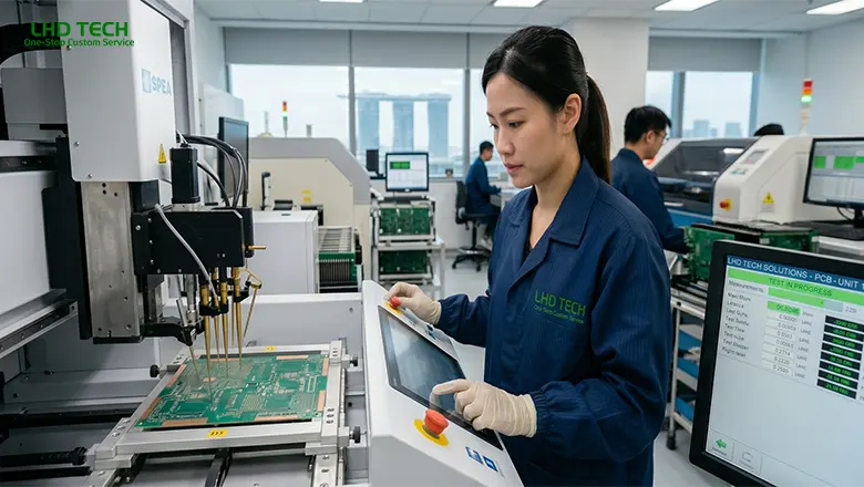
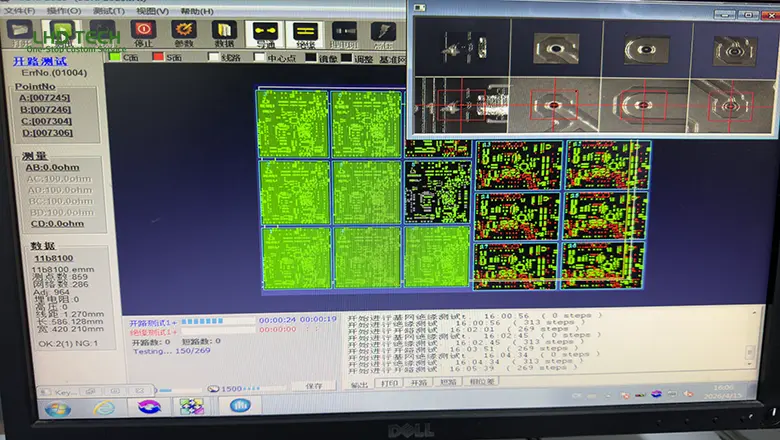
ICT (In-Circuit Test): High-Volume, Fixture-Based PCB Inspection
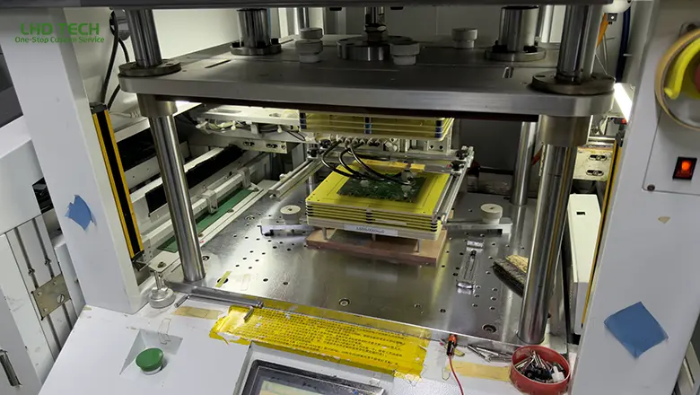
In-Circuit Test Explained
ICT, or In-Circuit Test, is a high-coverage, fixture-based test method suited for mass production. Using a bed-of-nails fixture, probes contact hundreds of points on the assembled PCB simultaneously. This enables rapid, automated detection of both assembly and process-related faults.
Typical Defects Detected by ICT
- Missing, swapped, or misaligned electronic components.
- Solder bridges, open pins, and functional faults at the net Incorrect resistor or capacitor values.
- The chip or microcontroller itself is faulty, or there is a programming error.
- Leakage, poor soldering, or short circuits—these cannot be detected by optical inspection.
Why Use In-Circuit Test for Production?
- High throughput: Once the fixture is made, ICT can process thousands of assembled PCBs per shift.
- Repeatable inspection: Software-controlled tests mean identical results for every board, driving robust process control.
- ROI: While fixture design costs are high, in large batches, ICT’s cost per PCB tested is extremely low compared to manual or probe-based methods.
Practical Example
A major consumer electronics contract manufacturer switched entirely from manual visual inspection to our deployed in-circuit test (ICT) solution for a batch of 100,000 PCBs. The results showed that the defect rate plummeted from 4% to below 0.3%, while overall testing labor costs decreased by 60%.
Automated Optical Inspection (AOI): High-Resolution Cameras for Defect Detection
AOI in Practice
Automated Optical Inspection (AOI) combines a high-resolution camera with advanced image processing algorithms to perform a visual “inspection” of the assembled PCBA. AOI excels in surface-level defect detection and enables rapid inspection in high-volume manufacturing and assembly lines.
What AOI Detects
- Solder bridges, solder voids, and insufficient solder on joints.
- Component polarity, missing or misaligned components.
- Deformation of leads, lifted pins, and coplanarity issues.
- Contamination or flux residue (to a limited degree).
AOI Best Use
- Post-SMT placement: AOI (Automated Optical Inspection) can quickly identify component placement and whether any components are missing.
- Post-reflow: AOI can detect component misalignment, tilting, and other minor soldering issues.
- Process improvement: The data provided by AOI can help us identify systemic problems early, such as the feed rate of the pick-and-place machine.
List: AOI Advantages
- Error rates lower than manual inspection.
- Non-contact, non-destructive, suited for fragile or densely packed PCBs.
- Fast reconfiguration for multiple PCB and PCBA types.
X-Ray Inspection: Non-Destructive Test Method for Assembled PCBs
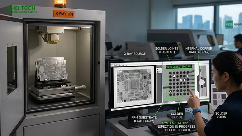
How X-Ray Inspection Works
For high-density assembled boards integrating BGA, QFN, and bottom-terminated components, traditional optical systems cannot penetrate them, necessitating X-ray inspection. X-ray images can clearly reveal hidden solder joints, internal interconnect structures, and variations in material density within multilayer boards.
X-Ray Test Method Covers:
- Solder joint voids and bridges under BGA balls or BTC terminations.
- Head-in-pillow defects commonly missed by other inspections.
- Hidden damage in buried vias and multi-layer traces.
- Lead frame delamination or internal contamination in ICs.
Example Use Case
A defense electronics company used X-rays to verify PCBs in a control prototype project. Before shipping, they discovered that the void rate of the BGA solder balls under the FPGA reached 3%, thus preventing the problem from occurring.
Boundary Scan Testing: Digital Integrity and PCB Inspection for Assembled PCBs
JTAG and Boundary Scan in Modern PCB Assembly
Boundary scan testing (often called JTAG testing) is a digital test method enabling defect detection in complex digital circuits without direct physical probe access. Test signals flow through a chain of enabled test logic inside integrated circuits, verifying communication, functionality, and even programming devices after final assembly.
Application Areas
- High-density, fine-pitch PCBs with many BGAs.
- Boards where fixture points are inaccessible.
- Debugging and functional test during both prototype and production.
What Boundary Scan Can Find
- Digital shorts/opens, pin connections, and programming issues with microcontrollers and programmable logic.
- Digital circuit integrity and inter-IC communication issues.
Functional Test (FCT): The Final Gate in PCB Assembly Testing
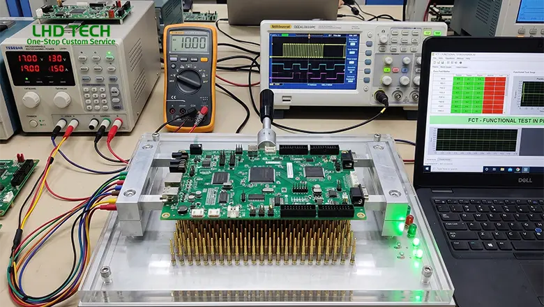
What Is a Functional Test?
Functional Test (FCT) puts the entire assembled PCB (PCBA) through its real operational cycles. FCT is the test that best simulates in-field use, running actual firmware and exercising all subsystems, from analog domains to high-speed digital interfaces.
Core Coverage of FCT
- Complete circuit and system-level functionality.
- Real input/output simulation and verification.
- Full power-up and power-sequencing validation.
- Board-level performance under thermal or electrical load.
Real-World Example
A communications infrastructure vendor saved $500,000 in potential field replacement costs by using FCT to stress-test assembled PCBs under hot/cold cycling, catching regulator failures that AOI and ICT missed.
Supporting and Extended Test Methods for PCB Assembly
Burn-In Testing for Reliability Assurance
Burn-in testing involves operating completed circuit boards under maximum temperature, voltage, and current for extended periods (often 48–168 hours). The goal is to expose “infant mortality” components and latent assembly defects that would otherwise escape even the most thorough functional test.
Best Practice
- For high-reliability products, such as medical equipment, automotive ADAS, and military electronics, aging tests can reduce maintenance costs.
Wetting Balance Analysis, Contamination Testing, and Manual Inspection
- Wetting Balance Analysis: Quantitatively measures solder wetting speed and “pull” – diagnosing contamination or poor solderability.
- Contamination Testing: Ion chromatography or ROSE testing is used to detect contaminants and flux residues on the PCB surface, as these factors directly affect the long-term reliability of the product.
- Manual Visual Inspection: For manually assembled prototype boards, rework stations, and scenarios that automated testing cannot cover, we often use manual visual inspection.
Choosing Effective PCB Testing Methods and Building Your Test Strategy
How to Select a Test Method for Your Circuit Board
- Prototype Circuits: Using flying probe testing combined with AOI offers fast line changes, high flexibility, and the best cost-effectiveness.
- High-Volume, Stable Boards: Using ICT with custom test fixtures, along with AOI to detect soldering issues, and FCT to verify system functionality.
- Complex/Multi-Layer Boards: X-ray and boundary scanning are used to discover hidden solder joint problems and faults in digital circuits.
- Critical Reliability Applications: These seven testing methods are used simultaneously, in addition to aging tests and some specialized functional stress tests.
Test Method Selection by Product Type
| Product Type | Recommended Test Methods |
| Prototype/Low-Volume | Flying Probe, AOI, Manual Inspection |
| High-Volume Consumer | Bare Board, ICT, AOI, FCT |
| Automotive/Military | Bare Board, ICT, AOI, X-Ray, Boundary Scan, FCT, Burn-In |
| Medical | AOI, X-Ray, FCT, Burn-In, Wetting Balance |
| HDI/Dense Digital | AOI, X-Ray, Boundary Scan, FCT |
Process Control, Quality Standards, and Continuous Improvement
Driving Ongoing Reliability in PCB Manufacturing
- Integrate Statistical Process Control (SPC): Collect defect data from each inspection or testing stage, and use data analysis to identify root causes and yield issues.
- Document and Retain Test Records: The testing equipment automatically records every result. These test records are used for warranty purposes and compliance traceability, especially for products meeting IPC Level 3 standards.
- Adjust Coverage Based on Failure Data: As production stabilizes, or if a certain type of field failure trend emerges in the product, we can flexibly adjust: making appropriate increases or decreases.
Case Studies: Successful Test Method Strategies in Electronics
Case 1: Flying Probe Prevents Prototype Disaster
A Silicon Valley IoT device startup avoided a $150,000 pilot-line delay by using flying probe and AOI to catch solder bridges and missing components on boards delivered for an investor demo.
Case 2: ICT+AOI Slashes Consumer RMA Rates
A large PC peripheral manufacturer dropped RMA rates by 75% after switching to full ICT fixture-based inspection and AOI, leading to a major retail contract win due to proven reliability.
Case 3: Automotive Board Survives the Toughest Test
A European ADAS system provider instituted a layered regime of bare board electrical test, automated AOI, and periodic X-ray. As a result, their boards achieved ISO 26262 certification with zero critical defects in two years of production.
FAQ: PCB Testing Method and PCB Assembly Testing
Q1: Can a single test method ensure total circuit board reliability?
A: No—maximum reliability requires layering multiple pcb testing methods to catch assembly, process, and design defects across all stages.
Q2: How do I verify my ICT fixture is working?
A: Run known defect “golden boards” and true-fault samples through your ICT station regularly, adjusting probe pressure and point targeting as needed.
Q3: Is AOI effective on every board type?
A: AOI (Automated Optical Inspection) excels in surface inspection, detecting issues such as misaligned or missing components, or solder bridging, especially on boards with high component density. However, AOI also has significant limitations—it cannot detect components like BGAs (Bottom-level Packages) or components with bottom terminations. AOI is typically used in conjunction with X-ray inspection and functional testing for combined checks.
Q4: When should I use flying probe vs. ICT in pcb testing?
A: For prototype boards, new designs, or small to medium batch production, chooseflying probe testing because it is flexible, responds quickly, and is cost-effective, making it a high-performance option for early PCBAs. In-Circuit Testing (ICT) is more suitable for high-volume production of boards with well-established designs. Although it requires more investment in test fixtures, its faster testing speed and higher coverage make it more cost-effective in the long run. For most mature designs, the optimal combination is: ICT + AOI + functional circuit testing.
Q5: How do I ensure compliance with IPC standards in my PCB assembly testing process?
A: Start by specifying the appropriate IPC class for your product application (Consumer, Industrial/Automotive, or High Reliability such as Medical or Aerospace). Work with your contract manufacturer to develop a testing and inspection plan that includes the required test method suite—bare board tests, fixture-based ICT, AOI, X-ray inspection, and boundary scan, as needed. Ensure that all processes are documented, test logs are retained, and periodic audits are conducted. Use checklists derived from the IPC-A-600, IPC-A-610, and other applicable standards to verify that assembly quality and defect criteria meet or exceed industry benchmarks.
Q6: What is the role of a functional test in overall circuit board reliability?
A: A functional test evaluates the assembled PCB under real-world operation, verifying that all systems, power domains, and I/O work exactly as intended. It’s the ultimate gatekeeper in PCB assembly testing, often catching intermittents, timing issues, and system-level faults missed by other methods. For mission-critical electronics, simulate environmental stress—as in power cycling, thermal cycling, or humidity testing—to expose failures that only emerge after shipment.
Key Takeaways: PCB Reliability Starts with Thorough Testing
- No single test method is enough: Use a combination of assembly inspection, electrical, and functional tests for the most effective pcb testing methods.
- Thorough testing throughout the life cycle—design, prototype, and production—builds reliability and reduces field failures and costly recalls.
- IPC standards are your blueprint: Let them guide the depth and rigor of every phase of manufacturing and assembly.
- Leverage high-resolution cameras, advanced probe technologies, and modern process control to catch evolving defect trends across all forms of electronics.
- Invest early in testability: Collaborate on test strategy, add test points and design for effective test coverage from the very first prototype.
Final Thoughts
In summary, high-quality and effective PCB testing methods are the difference between soldering success and silent, costly circuit failures. This guide to PCB, from flying probe and AOI to ICT and functional circuit testing, offers a holistic, reliable path to excellence in electronics. Whether you’re building one prototype or a million production boards, let the principles of fixture-based inspection, high-resolution cameras, data-driven process control, and thorough system-level testing guide every step. Your customers—and your bottom line—will thank you.