Introduction to PCB Assembly Drawings
Assembly drawings are far more than simple diagrams; each PCB assembly drawing is a technical document that translates design intent into actual manufacturing processes. In every modern printed circuit board assembly (PCBA) project, a well-designed assembly drawing is the bridge between design work and the actual manufacturing and assembly processes—without clear documentation, even the most innovative PCB designs can fail on the production floor.
PCB assembly integrates multiple disciplines—circuit design, placement, test engineering, PCBA, and even repair. Assembly drawings are crucial at all these stages, providing visual and data cues to ensure that every polarity mark, location, and solder joint is correct. For automated assembly lines, assembly drawings are essential for programming AOI (Automated Optical Inspection) systems and placement files. For manual assembly and rework, the assembly instructions translate complex requirements into actionable steps for technicians.
Why Assembly Drawings are Critical to PCBA
Assembly drawings are critical because they ensure the accuracy, repeatability, and cost-effectiveness of manufacturing and assembly—especially with the increasing complexity and component density of PCBAs.
The Role of Assembly Drawings:
- Visualize the assembly requirements and component positions and convey them to manual assemblers and automated systems.
- Coding assembly process rules: Advanced design rules from basic polarity and component orientation to 3D assembly and rigidity-flexible construction.
- Support for AOI system programming: By including detailed polarity markings and component profiles, AOI (Automatic Optical Inspection) verification becomes fast and clear.
- Transform design intent into assembly instructions: PCB assembly instructions, whether general or specific, bring the original design files from the screen to the real world.
- Reduce errors: They prevent costly errors in polarity, orientation and assembly processes, directly contributing to improved reliability.
Why Are Assembly Drawings Often The Most Important Document in the Package?
- Maintain assembly drawings: The accuracy and reliability of the entire design depend on them.
- Avoid expensive NPI/DFM errors, field failures, and confusion about component orientation or special assembly instructions
When a PCB manufacturer, PCBA house, or repair technician can rely on your assembly drawings, your finished product is more likely to succeed in the market.
PCB Assembly Drawing vs. Fabrication Drawing
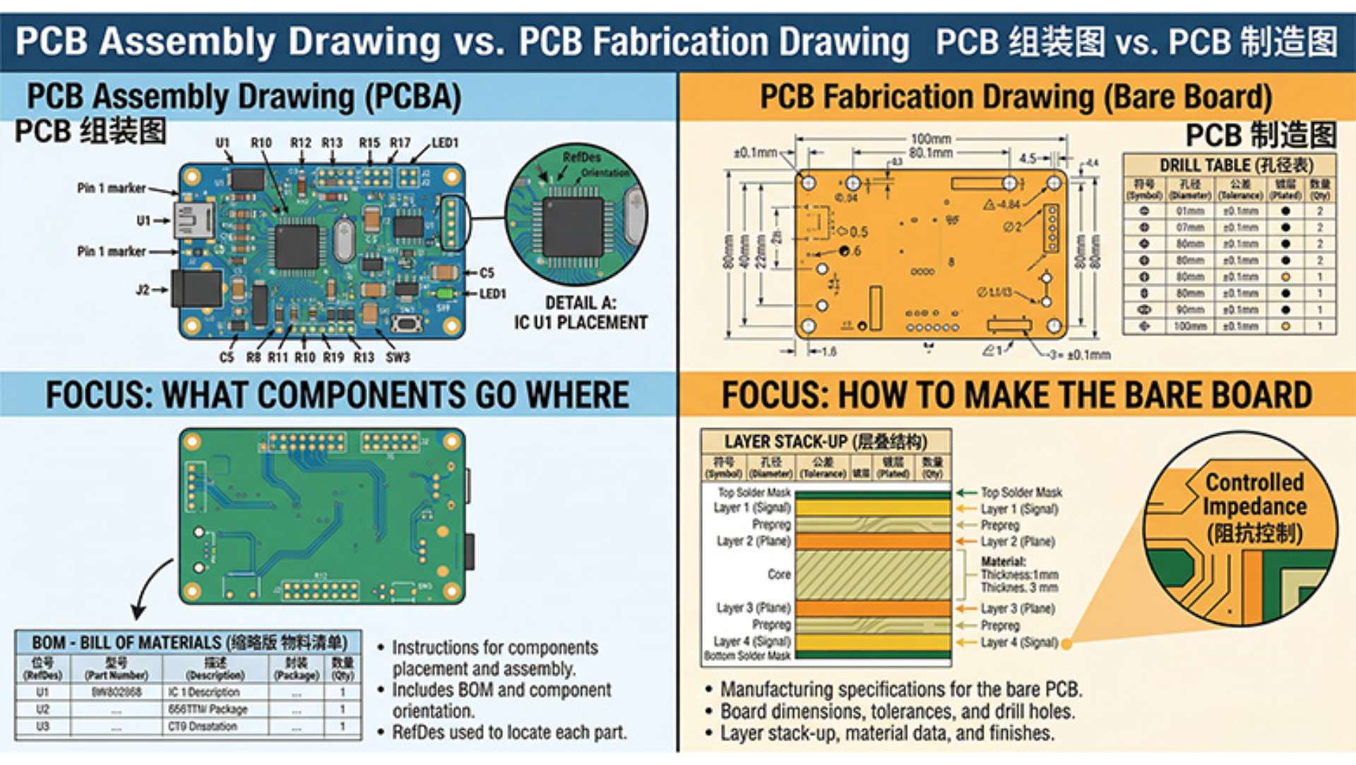
Although their names are similar, pcb assembly drawings and pcb manufacturing and assembly drawings are fundamentally different technical documents. This distinction is at the core of successful manufacturing and assembly.
Fabrication Drawing
- Documents how to fabricate the bare PCB (no components).
- Includes mechanical details: PCB outline, hole patterns, solder mask, copper layers, and silkscreen layers.
- Used by the PCB manufacturer for board fabrication, not for assembly.
PCB Assembly Drawing
- Tell how to assemble a bare PCB into a functional PCB and pcba.
- It contains all the information required for placing, positioning and welding each component.
- The core of the assembly process guides all the work from the initial placement to the final inspection.
Key Differences
| Document Type | What It Covers |
| Fabrication | Board outline, stackup, drills, copper, silkscreen |
| Assembly Drawing | Component locations, polarity, assembly notes, 3D |
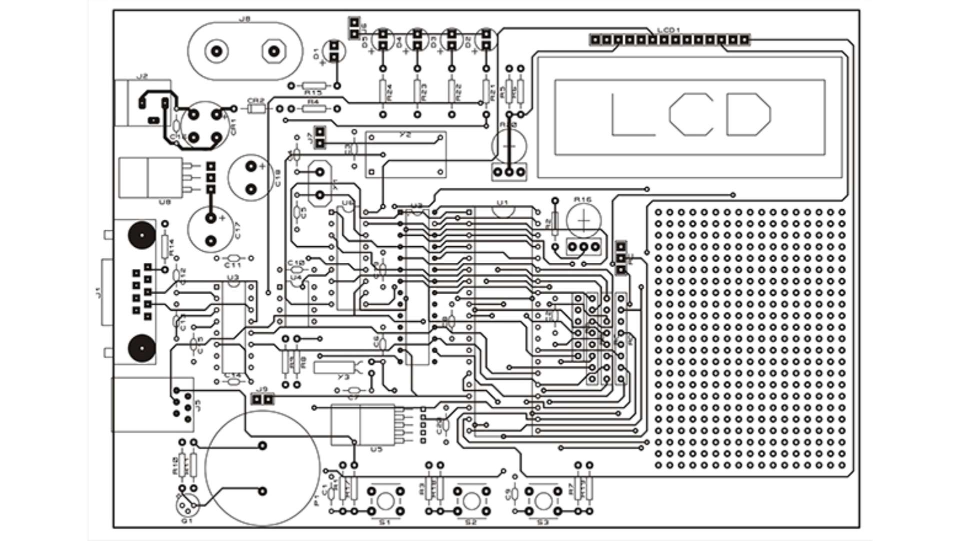
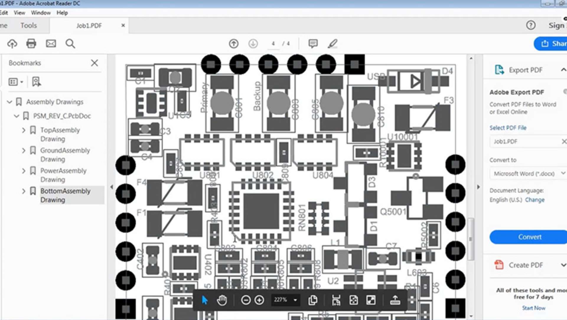
What an Assembly Drawing Contains
Professional pcb assembly drawings tell your manufacturing partners almost everything needed to assemble the entire design and serve as the main technical guide during the assembly process.
A complete assembly drawing contains:
- Top and bottom panel views, each with clear reference signs
- Component profile and placement marking (suitable for automatic assembly and manual placement)
- Pin 1 and polarity marking, especially for ics, polarized capacitors (such as electrolytic capacitors) and diodes
- Benchmark to keep the AOI system consistent with the SMT line
- Assembly instructions section (including specific component requirements, PCB assembly instructions and process marks)
- Equal-length /3D assembly view (for rigid-flexible/complex/advanced PCB design)
- Silk-screen printing and assembly layer marking for rapid visual verification
- Detailed views/annotations of high-density or risk-prone sections (e.g., BGAs, qfn, micro-BGAs or through-hole mounting)
- Mechanical hardware, the position and precautions of crimping connectors or test points
Core Assembly Drawing Elements
1. Reference Designators, Marking, and Component Locations
- Each component must have a reference identifier that matches the BOM and the pick-and-place file.
- The polarity or pin 1 marking must be large, clear, standardized IPC-D-325 and IPC-A-610.
- High-density areas should be marked, and if possible, detail views or 3D views should be used.
2. Polarity, Component Orientation, and Placement
- Use clear symbols (+,-, dot, arrow) to indicate the orientation of capacitors, diodes and ics.
- For advanced designs, if specific components have unusual requirements (for example, hot pads, key gate drivers), always include descriptions.
- Through-hole and SMD components, such as electrolytic capacitors or BGAs, require clear orientation instructions.
3. 3D Assembly Views and Advanced Details
- For multi-board or rigid-flexible components, use the 3D component view in pcb design software to display spatial relationships and capture mechanical conflicts before construction.
- These viewpoints are becoming increasingly important for wearable, industrial or IOT where every millimeter counts.
4. Assembly Notes, BOM, and Place Files
- Assembly notes are operation notes: handling precautions, solder type, cleaning, inspection steps or process sequence.
- Bill of Materials (BOM) : Directly link each identifier and footprint in the pcb assembly drawing to procurement, testing, and replacement.
- Placing files (pickand placing file) : Precise X/Y/ rotations used in SMT machines and AOI programming.
5. Process, Reliability, and Special Assembly Instructions
- There are good assembly annotation section marks where additional process attention is required (for example, manual welding, anti-static, double reflow soldering, and crimping).
- Provide concise reliability information: Is core blockage prone to occur in this area? Is special testing required? Are there controllable impedance lines?
- Pay attention to any DFM/DFT checkpoints, part replacements, or the test fixtures used.
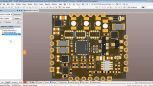
How To Generate Assembly Drawings in PCB Design Software
Modern electronic design automation (EDA) tools, such as Altium Designer, KiCad and Cadence Allegro, have the powerful function of generating assembly drawings directly from PCB design files. This simplifies DFM and ensures that the manufacturing and assembly teams always work in accordance with the true design intent.
General Steps (Applies to Tools Like Altium, KiCad, Cadence, and More):
- Complete your PCB design: Ensure that all reference indicators, footprint allocation and orientation details in the PCB design tool are correct. Carefully check the footprint, polarity and orientation of each component in the circuit layout.
- Select layer export: Activate the assembly layer (not just silk-screen) in the pcb design software. Many design teams make the mistake of only placing component Outlines in the silk-screen layer, resulting in incomplete assembly documentation. Use the precise footprint of the assembly layer, polarity marking, and special assembly instructions.
- Prepare 3D assembly views: Advanced PCB design tools such as Altium enable you to generate 3D assembly views, showing component height limits, mechanical fits, or interference with the housing. These 3D views are indispensable for complex boards, rigid-flexible designs or multi-board assemblies.
- Insert assembly instructions and special notes: Each assembly drawing should have an annotation section that includes specific assembly requirements, PCB assembly instructions, ESD warnings, cleaning or solder paste details. This section ensures that even the tiniest details are conveyed to the assembly line, whether they are automatic or manual.
- Cross-reference with BOM and centroid (pick-and-place) files: The assembly drawing provides a visual map. Use BOM and centroid/position files (generated in tools such as Altium, KiCad, or OrCAD) to align each reference indicator, component orientation, and exact position.
- Version control and final review: Before release, ensure that the assembly drawing, BOM, Gerber file, and place file all refer to the same version/revision. Good assembly documents are always under strict version control to track changes and avoid confusion in the workshop.
- Export document: Modern PCB design tools allow you to export PDF for human reading, as well as formats such as odb++ /IPC-2581, for automatic login to AOI, SMT or test systems.
Advanced Design: 3D Assembly Views, Rigid-Flex, and HDI
As miniaturization and multi-functionality dominate electronic design, advanced assembly drawing capabilities are essential.
Why Use 3D Assembly Views?
- Detect mechanical conflicts: The 3D assembly view visualizes the interaction of components such as high electrolytic capacitors or heat sinks during the final assembly.
- Visualized segmented assembly: For rigid or stacked PCBS, 3D views guide technicians to complete multi-step assembly and folding.
- Communicating with non-designers: Managers, test engineers, and CMs may lack a complete ECAD license, but they can easily understand the design intent.
Rigid-Flex and HDI PCB Assembly Drawing Requirements:
- Each rigid and flexible part of the label. Use arrows and color codes to indicate curved areas and no-position areas.
- Specify unique assembly process steps (such as the assembly sequence of through-holes and SMT components).
- Highlight any requirements that are only rigid and flexible, such as “welding reinforcing agent before flexible folding” or “no solder paste in the flexible area”.
Assembly Notes, Special Instructions, and BOM
What Makes Assembly Notes Effective?
- Be clear: Do not write “Handle with care”, but “Manual welding of U5 after AOI”. Comply with anti-static precautions; Polarity markings are shown in the assembly drawing.
- Link to the reference indicator: Use markings such as “D3, D7 – Verify that the cathode marking is aligned with the assembly drawing before welding”.
- Preventing process errors: Precautions should warn sensitive components, areas that require additional solder paste, or oddly shaped components that may not be suitable for automated assembly.
- Coordination with BOM: Directly record any replacement parts, value changes or “Do not Place” (DNP) components in your notes.
BOM in Assembly Drawing Context
Each assembly drawing must conform to the BOM (Bill of Materials). For each component, the BOM should include:
- Designator
- Part number and description
- Value and packaging (including through-hole or SMT
- Supplier or approved alternative information
- Polarity (if applicable)
- Quantity per board
- Specific assembly instructions (for example, “DNP for Version B boards only”)
| Ref Des | Part Number | Description | Value | Package | Qty | Notes |
| C1 | ELEC-16V-10uF | Electrolytic capacitor | 10uF | SMD | 1 | Observe polarity |
| U2 | IC-MCU-ATSAMD21 | Microcontroller | — | QFN48 | 1 | Solder center pad |
| J1 | CONN-USB-A | USB connector | — | TH | 1 | Hand solder only |
Good Assembly Practices & PCB Assembly Notes
Whether your circuit board is for the first prototype or production run, a good PCBA always starts with strict documentation.
What Does Good Assembly Mean?
- Each polarity mark is clear and matches the silk-screen printing and schematic diagram.
- The BOM, centroid and assembly drawing always match the revised version.
- The assembly instructions (manual or automatic assembly) are clear, concise and operable.
- 3D assembly view, suitable for high-density, stacked or advanced designs.
- The assembly instructions list every inconspicuous instruction (for example, mechanical preloading, post-weld cleaning, operational restrictions).
Frequent Pitfalls to Avoid
- The device direction is not clear (for example, SMD led with non-standard pin 1)
- Missing or ambiguous assembly comment sections.
- Failure to update the drawings and BOM simultaneously (resulting in on-site support issues)
- Use the old silk-screen layer that conflicts with the data of the new assembly layer.
Typical Assembly Process and Design for Manufacturing
Assembly Process at a Glance
- Stencil & Solder Paste Application: Solder paste is applied to SMT pads according to the pcb design file.
- Component Placement: Automated and/or manual placement guided by the assembly drawing and pick-and-place file.
- Soldering (Reflow & Through-Hole): All SMD components are reflow soldered; through-hole and special assemblies are usually hand or wave soldered as per assembly notes.
- Inspection (AOI/AXI Systems): The assembly drawing provides the visual reference for automated optical and X-ray inspection system programming.
- Testing (FCT/ICT): Engineers use the assembly drawing, test fixture documentation, and assembly notes as a troubleshooting map.
Design for Manufacturing (DFM):
- Generate the assembly drawing as early as possible and communicate with the PCB manufacturer about any unique or risk-prone areas.
- Before release, use electronic design automation tools to check for component collisions, polarity errors or lost data.
- Assembly drawings provide important clues for the manufacturing process and comply with the principles of DFM and DFA (Assembly Design).
Assembly Drawing as the Bridge in the Manufacturing Process
It’s not just about documentation: Assembly drawings tell the assembly workshop how to transform your design intent (what you see in the pcb design software) into a working, testable and reliable pcba.
- The design team conducted a preliminary review using assembly drawings.
- PCB manufacturers use it to program their AOI, SMT and test lines.
- Assembly technicians and maintenance teams use it for inspection, rework and continuous support.
- On-site service refers to troubleshooting several decades after the prototype is launched.
When modifications are needed, the assembly drawing serves as a technical record of these changes and also acts as a reference standard for on-site installation.
Automated Assembly, AOI, and Assembly Drawing Capabilities

Automated Assembly and Good Assembly Drawings
- PCB assembly drawings are particularly important for automated assembly: the better your drawings are, the fewer problems and downtime there will be on the automated production line.
- Generating good assembly drawings can optimize feeder Settings, reduce the ambiguity of the visual system, and ensure precise picking even in challenging component directions.
AOI, AXI, and Assembly Drawing Capabilities
- AOI system programming depends on polarity marking and the correct component placement data from your assembly drawing and placement files.
- AOI and AXI test the entire circuit based on these markings; Mismatches are immediately marked and rework is allowed before the final test.
- Good assembly reduces manual intervention and increases output.
Common Mistakes in PCB Assembly Drawing and How to Fix Them
Checklist of Frequent Mistakes
- Things that fail to mark polarity or direction, such as electrolytic capacitors.
- Omit the annotation part or use unclear language.
- There is no reference to each specific component in the BOM, drawings, and centroid/position files.
- For components with unclear directions, the detail view is omitted.
- Using outdated silk-screen layers or failing to update the assembly layers after design changes.
- The assembly instructions for unique or sensitive components are unclear or missing.
- For rigid-flexible, stacked or mechanically constrained designs, the 3D assembly view is insufficient or missing.
- Skipping version/revision control – resulting in a mismatch between BOM, assembly drawings, and pick-and-place files.
- Before the assembly drawing was released, it was not reviewed together with the manufacturing/assembly team.
How to Fix and Prevent These Issues
- Establish a review process: Each assembly drawing should be reviewed not only by designers but also by manufacturing, assembly and testing engineers. This multidisciplinary feedback highlights the ambiguity and absence of pre-release data.
- Automated consistency check: Use PCB design software functions or custom scripts to cross-check for missing or mismatched reference indicators and marks in your BOM, assembly drawings, silk-screen printing, and centroid files.
- Maintain strict version control: Update the assembly drawing whenever there are changes in the BOM, component layout or specific assembly instructions, and synchronize the file versions in all package documents.
- Provide details and 3D views: For dense PCBS, advanced designs (HDI), through-holes or rigid-flexible builds, 3D assembly views and detail callouts in the drawings can prevent expensive prototype rework.
- Keep assembly notes up to date: Update the assembly note section to include on-site feedback, test failures, and input from assembly technicians, not just design assumptions.
- Communicate with your product manager: Ask your contract manufacturer to review your documents before production and state their feedback in your assembly drawings and notes.
Case Study: Assembly Drawing for a Complex Modern PCBA
Let’s consider the “Orion Project” – an Internet of Things sensor node designed for environmental monitoring, featuring rigid-flexible PCBS and a high-density component layout.
Requirements:
- It occupies a small area and is equipped with stacking plates and through-hole connectors
- Sensitive analog front ends require special ESD and soldering process steps
- Rapid scaling from prototype to batch PCBA is required, along with automated assembly
PCB Assembly Drawing Solution:
- Generated in Altium, it includes clear views of the top and bottom assembly layers, explicit polarity and orientation markings for each IC and capacitor, as well as clear marking positions for all specific components.
- It provides a 3D assembly view, showing how the curved and rigid parts align and fold within the final housing.
- The BOM, pick and assembly instructions sections are all revised, locked and machine-readable, and incorporate the latest feedback from the prototype stage.
- Assembly precautions: “Connector J3 should remain unsoldered until it is inserted into the circuit board.” Then through-hole welding and the final test.
- Special assembly instructions for the simulated front-end area: “Wuxi Paste near U6.” Weld by hand in accordance with AOI requirements and inspect under a microscope.
- Quickly incorporate on-site support and the feedback from the first batch of production, update the PCB assembly instructions, and provide better assembly processes for mass production.
Conclusion: Assembly Drawings for Quality and Reliability
A pcb assembly drawing is not merely a technical document: it serves as a bridge spanning the complex world of design and manufacturing. Each circuit, BOM entry and detail in the assembly drawing will enhance the reliability, speed and quality of the entire design process.
Key Points:
- Based on the latest BOM, location files and PCB design data, create and maintain detailed, consistent and clear assembly drawings.
- Use assembly drawings to convey each specific assembly requirement, the position, orientation, polarity and process description of components.
- Including 3D assembly views and detail/insert views in advanced or dense layouts.
Leverage the capabilities of modern electronic design automation tools, such as Altium, KiCad, Cadence, and other drawing generation and data synchronization.
- Practice manufacturing design by involving the manufacturing and assembly teams as early as possible and responding to their feedback.
- Support every manufacturing stage, from prototyping and maintenance to mass production and on-site service, and provide reliable version control documentation.