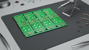
Introduction to PCB Fabrication
Every electronic device you rely on—from smartphones to aircraft navigation systems—depends on a precise, multi-stage pcb fabrication process. This article explores every essential aspect of how a circuit board design becomes a physical structure supporting electronic components. For product designers and engineers, understanding the pcb fabrication andpcb assembly process is crucial to achieving optimal product performance, reliability and manufacturability.
As technology and demand evolve, so must the techniques we use to fabricate printed circuit boards (PCBs). The journey from pcb design and computer-aided design (CAD) through pcb production and assembly involves several steps. Each step in the process is critical: quality check protocols, regulatory requirements and new material trends all impact the finished circuitry.
Key Highlights of the PCB Fabrication Process
PCB fabrication is the process that converts digital blueprints into working, manufacturer-ready circuit boards. Whether you’re designing a simple LED board or a multilayer Taconic PCB for RF applications, the process involves:
- Transforming board design into a physical structure;
- Following strict design specifications and industry standards;
- Adapting to the required number of layers and design requirements (from single layer to complex, high-speed multilayer circuits);
- Integrating quality checks at every stage of PCB production to prevent short circuits, opens and physical or chemical defects.
Overview of the PCB and Its Role in Electronics
A printed circuit board (PCB) is the backbone of modern electronics. It provides electrical pathways and mechanical support for electronic components in everything from consumer gadgets to industrial equipment. The entire PCB consists of:
- A base substrate (FR-4, Rogers, Taconic, aluminum)
- Multiple thin layers of copper (usually rolled copper foil)
- Solder mask to protect the copper and signal traces
- Silkscreen for labels and identification
- Vias, pads and drilled holes for both through-hole and surface-mounted components
Overview of the PCB:
| Layer/Section | Function |
| Substrate/Core | Mechanical support |
| Thin Layer of Copper | Conductive traces, pads, and vias |
| Solder Mask | Protection, prevents solder bridges |
| Silkscreen | Markings, component ID, assembly assistance |
| Resin (Prepreg) | Cross-linking structure in multilayer PCBs |
What is PCB Fabrication? Full Overview

PCB fabrication is the process of creating the bare board from a digital design, primarily transforming the circuit board design into a physical structure. It includes:
- Photolithography and photoresist application;
- Drilling and plating process for creating conductive interlayer vias and component holes;
- Solder mask application to protect the copper;
- Silkscreen printing for readable identification;
- Implementation of all stack-up and pcb design.
PCB Fabrication Process vs. PCB Assembly Process
| PCB Fabrication Process | PCB Assembly Process | |
| Main Focus | Making the bare board, copper layers, vias | Soldering electronic components to the board |
| Output | Bare board/physical structure | Assembled, working product |
| Quality Check | Electrical test, AOI, microsection | In-circuit test, x-ray, functional test |
| Steps Involved | Up to 20+, from imaging to final inspection | Paste printing, component placement, soldering, AOI |
Difference between pcb fabrication and pcb assembly: The manufacturing phase converts CAD files into physical circuit boards, while the assembly phase solders and secures electronic components onto the boards.
Pre-Fabrication: Design and Planning

The entire manufacturing process of printed circuit boards is officially launched by a professional design team.The design team employs computer-aided design CAD tools to conduct precise planning and complete design for the overall structure of the circuit board.The various preparatory tasks prior to the formal start of manufacturing procedures specifically include:
- Checking DFM (Design for Manufacturing), ensuring board design can be reliably manufactured;
- Checking the number of layers, minimum trace widths, via types and keeping within manufacturing tolerances;
- Exporting Gerber files and netlists—essentials for communicating design requirements to the fab house;
- Creating a complete Bill of Materials (BOM);
- Reviewing for any potential PCB defects before initiating production.
Best Practices:
- Work closely with your PCB fabrication partner in the pre-fab stage.
- Run a DFM review and address all manufacturability issues early to avoid costly respins during production.
Step-by-Step PCB Fabrication Process

The pcb fabrication process involves several steps, each of which is critical to the board’s structural and electrical performance.
1. Photolithography: Photoresist and Imaging
- A thin layer of photoresist, either as a liquid or dry film, is applied to the copper foil surface of the entire PCB.
- The circuit pattern is printed onto the boardusing UV light in a design-specific mask.
- Exposed areas are then developed, washed and dried for further processing.
2. Etching and Rinsing
- The pattern exposed via the photoresist is chemically etched away, removing unwanted copper and leaving behind only the correct trace layout as per the CAD design.
- Boards are rinsed and inspected for etch residues.
3. Layer Alignment and Inner Layer Bonding
- Multilayer fabrication processes require stacking several layers of the PCB, separated by resin-rich prepreg.
- Alignment marks ensure every layer matches the computer-aided design.
- The layers are pressed and cured, forming the stacked board.
4. Drilling of Holes and Vias
- Holes are drilled where vias or through-hole pads on the PCB are needed, as well as to accommodate electronic components.
- Drilling can be done by CNC machines or lasers (for microvias).
- Holes are cleaned to remove resin smears or burrs.
5. Electroless Copper Deposition
- A thin layer of copper is deposited chemically onto the drilled hole walls, prepping for further reinforcement via the electroplating process.
6. Electroplating Process
- Copper using an electroplating process is applied to the entire PCB and especially onto the hole walls, building up sufficient thickness for reliable interlayer connections.
- Plating thickness is carefully controlled according to design specifications.
7. Outer Layers of the PCB
- Outer layers are similarly imaged and etched, with their own photoresist steps and UV exposure.
- Additional electroplating thickens pads on the PCB and surface traces.
8. Solder Mask Application
- a solder mask is applied to the PCB surface, typically using liquid photoimageable materials, though dry film is also an option. This coating covers the copper foil on the outer layer circuitry. It protects copper traces from oxidation and corrosion, while also preventing short circuits caused by solder bridging during the assembly process.
- after application, the solder mask is selectively cured/hardened using uv light, covering everything except selected pads where electronic components will be soldered.
- this stage of the pcb process is crucial for ensuring pcb quality, as improperly applied solder mask can lead to electrical shorts and field failures.
9. Silkscreen Application And Surface Finish
- next, a silkscreen layer is printed onto the board. this layer provides essential component designators, polarity marks, part numbers and assembly cues. good silkscreen ensures that during the assembly stage, technicians and machines can accurately place components.
- following silkscreen, the pcb receives a surface finish. popular finishes include:
- hasl (hot air solder leveling): affordable, robust but not ideal for ultra-fine designs.
- enig (electroless nickel immersion gold): provides a smooth, solderable surface, excellent for high-density boards.
- osp (organic solderability preservative): eco-friendly, lead-free.
- immersion tin/silver: selected for specific compatibility or high-frequency use.
- the finish is chosen based on the pcb design, assembly requirements and end-use environment.
10. Final Shape: Routing, V-scoring and Beveling
- the entire pcb (or a panel of boards) is cut into its desired shape using cnc routers. boards may also receive v-grooves (scoring) for easier separation after the assembly process.
- beveling is applied to edge connectors for improved insertion and longer lifespan.
- the process involves several steps of mechanical and visual quality check, ensuring no damage or burrs exist on the finished boards.
11. Electrical And Automated Optical Inspection (AOI)
- before shipment, every bare board must pass thorough quality checks:
- electrical test: checks for opens, shorts, and correct net connections by probing every trace and pad on the pcb.
- automated optical inspection (aoi): high-speed cameras compare every manufactured board against the original computer-aided design for misalignments, missing features or unexpected deviations.
- x-ray inspection may also be used for dense, multilayer pcbs.
- this stage is vital for catching errors not visible to the eye, such as breaks in inner layers of the pcb.
12. Packaging And Shipping
- after passing all inspections, pcbs are de-panelized if needed, cleaned and packaged in moisture-barrier and esd-safe materials.
- labels for pcb production traceability and compliance (such as rohs, itar or ul marks) are applied.
- shipping in controlled atmosphere packaging preserves pcb quality until the assembly stage.
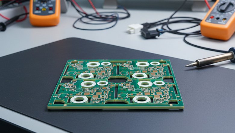
Key Parts And Layers Of The PCB In Fabrication
Designers must clarify the function of each copper foil layer; manufacturers must also master the lamination sequence and thickness specifications of all layers. A multilayer printed circuit board is constructed by alternating stacked conductive circuit layers and insulating material layers.
| layer | purpose |
| substrate (core) | provides the mechanical/physical structure using fr-4, rogers, or taconic pcb materials |
| thin layer of copper | used for signal and power routing, one per layer |
| prepreg/resin | bonds layers, ensures dielectric separation, and supports lamination |
| solder mask | protects copper, defines solder areas |
| silkscreen | guides assembly, helps identification |
each layer is created, aligned, and inspected. the quality check of layer registration is a crucial process: even a 50-micron shift can cause short circuits or open connections, especially in high-pin-count designs.
Main Challenges And Considerations In The PCB Fabrication Process
the pcb fabrication process involves several steps and challenges, including:
- PCB manufacturing must strictly follow the standards set during the computer-aided design stage.Parameter requirements including trace width, spacing and drill diameter marked on the design drawings shall be fully implemented in the production process.
- selecting compatible materials: High-frequency circuit boards mainly adopt Rogers or Taconic materials in material selection.High-power applications have special requirements for copper foil thickness, and thicker specifications are usually adopted.
- ensuring dfm—design for manufacturing—is considered to avoid costly respins.
- The dimensions of vias and traces must be strictly controlled.Even extremely minor dimensional deviations can lead to energy attenuation during signal transmission, ultimately resulting in signal loss or connection failure.
- robust quality check at every stage, from dry film alignment to final inspection.
- environmental compliance: processes must follow rohs and, in some cases, itar regulations.
PCB Fabrication vs. PCB Assembly
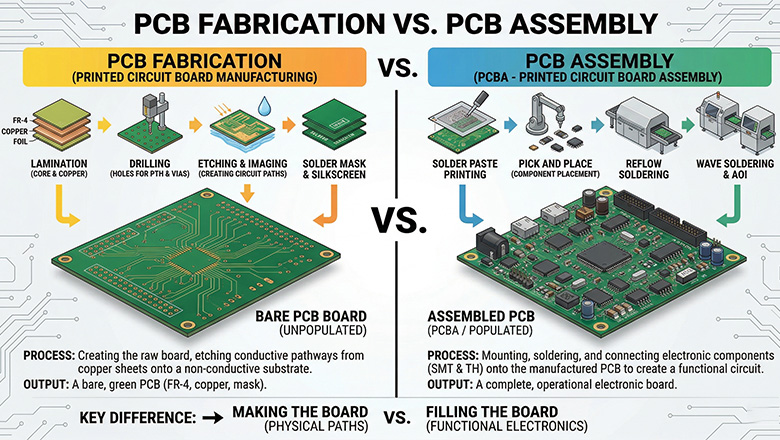
Understanding The Difference Between PCB Fabrication And PCB Assembly
- pcb fabrication is the process of turning the board design into a physical structure—building the bare board itself with all required layers, copper traces, drilled holes and finishes.
- pcb assembly (sometimes called pca or printed circuit board assembly) is the process that follows fabrication. it involves attaching and soldering electronic components onto the bare board.
- the fabrication and pcb assembly process often interact; poor fabrication can jeopardize component placement, soldering quality, and product reliability.
- for full turnkey projects, your partner may handle both pcb fabrication and pcb assembly under one roof for a streamlined, quality-controlled process.
How To Implement And Optimize PCB Fabrication Processes
Practical Steps And Optimization Tips
- start with a robust pcb design: use advanced computer-aided design tools and run thorough dfm reviews.
- always specify critical tolerances: minimum annular ring, via aspect ratio, edge clearances, copper thickness.
- choose fabricators with modern equipment: those using ldi, laser drilling, and real-time aoi deliver higher reliability.
- request test coupons and detailed inspection reports: these help verify that the production batch matches your design requirements.
- for sensitive applications: consider extra quality check protocols such as ionic contamination testing, cross-section analysis and even reliability testing for automotive or aerospace pcbs.
- collaborate often: keep communication open between your design team, fab house and assembly partner.
Choosing The Right PCB Fabrication Partner
What To Look For In A Good PCB Manufacturer
- breadth of fabrication processes supported (ldi, hdg, impedance, via types, etc.)
- real-time status tracking and quality data for each batch
- compliance with industry standards (ipc, ul, rohs)
- transparent quoting—including all process details, tolerances, and delivery timelines
- clear communication and willingness to advise on dfm optimizations
Tips For A Successful PCB Fabrication Project
- share your entire pcb design, including netlist and layer stack-up, not just gerber files.
- clarify the number of layers, via type (buried/blind), critical trace widths, target impedance, and all design specifications.
- request a dfa/dfm review before final board fabrication.
- integrate your supply chain: ensure your assembler and pcb supplier are aligned on panelization, stencil design and fiducial placement.
- for rapid prototyping, choose partners with quick-turn capabilities.
- always document any deviations from standard processes agreed upon.
Frequently Asked Questions About PCB Fabrication
Q: how many steps are in the average pcb fabrication process?
A: typically, a minimum of 15–20 steps, including imaging, etching, drilling, plating, surface finishing, aoi/inspection and final cleaning and packing.
Q: how is computer-aided design (cad) used in the process?
A: cad files define every aspect of the pcb from layout to holes to solder mask. these files drive all automation and inspection throughout fabrication.
Q: what’s the difference between the fabrication and assembly stage of pcb production?
A: fabrication creates the bare board, while assembly attaches electronic components using processes like smt, wave solder and through-hole insertion.
Innovations And Trends In PCB Fabrication Processes
- digital manufacturing: connects cad, mes (manufacturing execution systems) and erp for seamless design-to-fab automation.
- advanced photoresist: new dry film and lpi formulations improve edge definition for fine-pitch circuit boards.
- green chemistry: rohs-compliant processes reduce hazardous waste and improve workplace safety.
- additive pcb manufacturing: selective material deposition instead of subtractive etching for lower waste and rapid prototyping.
- ai in inspection: modern aoi systems use machine learning to detect subtle defects beyond human perception.
Case Studies: Real-world PCB Fabrication Examples
example 1: a medical device company’s design team needed a dense, 10-layer taconic pcb. their fabricator’s agile fabrication processes, including x-ray aoi and cross-section testing, ensured zero short circuits or etching defects across 2,000 sample boards.
example 2: an automotive supplier optimized their assembly process after discovering that etch-back and resin void quality checks in the fabrication process drastically reduced field failures in power circuit pcbs.
Glossary of Key PCB Fabrication Terms
- fabricate: To make or construct a physical printed circuit board from design files through the pcb fabrication process.
- pcb fabrication process: The series of fabrication processes that transform circuit board design into a bare board substrate for assembly.
- pcb assembly process: The stage where electronic components are mounted and soldered onto the fabricated board.
- photoresist: Light-sensitive material (applied as liquid or dry film) used to image the design onto copper foil layers during photolithography.
- layers of the pcb: The stack-up of substrate, copper, solder mask, resin and silkscreen, defining the entire PCB’s physical and electrical structure.
- dry film: Pre-coated, solid form of photoresist used in the imaging process to deliver sharper definition, crucial for fine-pitch circuits.
- deposit: The application, by chemical or electrochemical means, of a thin layer (such as copper using an electroplating process) for conductive and protective purposes.
- pad: Copper area on the board for connection of component leads or via structures.
- trace: Conductive copper line on a PCB, connecting electronic components.
- etch/etched away: The chemical process of removing excess copper from the board, leaving the designed circuit pattern.
- computer-aided design (CAD): Software environment used for schematic entry, pcb design layout, and generation of fabrication data (Gerber files).
- quality check: Inspection processes (such as AOI, electrical test) applied at various steps to ensure zero defects in the final board.
- difference between pcb fabrication and assembly: Fabrication refers to bare board creation; assembly is the process of populating the board with electronic components to create the finished printed circuit board assembly (PCBA).
- number of layers: Reflects the complexity of the pcb design; high-performance boards may use 4, 6, 10, or even 32 layers.
- dfm: Design for Manufacturing—set of guidelines that help adapt pcb designs for efficient, defect-free fabrication and assembly.
Conclusion: The Critical Nature of PCB Fabrication
The pcb fabrication process transforms your circuit board design—created with sophisticated computer-aided design tools—into a tangible, robust substrate, prepared for assembly and market success. As you’ve seen, the process involves several steps, from photoresist coating, imaging, and etching, through drilling, copper deposition, and multi-stage quality check routines, to final solder mask application and silkscreen marking. Each of these fabrication processes is vital to produce a high-quality, reliable PCB that meets demanding electronic, mechanical and regulatory requirements.
Understanding the difference between pcb fabrication and pcb assembly allows design teams to anticipate and avoid common pitfalls, ensuring that design specifications translate into reliably manufactured products. Whether you’re launching a new IoT device or designing mission-critical aerospace controls, proactive DFM collaboration and process transparency with your board fabrication partner will speed your time-to-market, reduce cost and boost overall board quality.