Introduction: PCB V-Scoring and Printed Circuit Board Assembly
PCB v-scoring is a critical process in modern pcb manufacturingandassembly. Whether you’re designing a pcb prototype or running a high-volume production line, efficient circuit board separation methods have a direct effect on cost, structural integrity, and board reliability. V-scoring uses precise, V-shaped grooves (or “scores”) along defined lines of a pcb panel, creating partial cuts to facilitate the separation of multiple pcbs after assembly.
This technique is foundational in creating smooth edges and allowing for the fracture-free breaking apart of boards, much like snapping pieces from a chocolate bar. By using controlled score lines, pcbs can be separated with minimal stress on the board and components, maintaining the high standards necessary in today’s advanced electronics manufacturing markets.
What is a V-Score? The Role of V-Shaped Grooves in PCB Boards
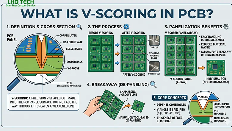
A V-score is a linear, V-shaped groove etched into the surface of a printed circuit board panel. These grooves are made using a V-shaped cutting tool that removes material from both the top and bottom surfaces, but not all the way through. The remaining web of pcb material in the middle holds the panel together, with a thickness carefully calculated to ensure stability during assembly, but easy breaking post-assembly.
V-Scoring reduces the material between adjacent pcbs, letting you maximize panel utilization.
Analogy: Think of a chocolate bar—deep, narrow grooved lines allow you to break the bar into perfect squares, with little force and no crumbling. V-scoring achieves this for your circuit boards.
- V-scoring usesa V-shaped cutting wheel to create the grooves.
- The score angle and depth are determined based on panel thickness and assembly needs.
- Panels with V-scores can be broken apart by hand, with a pizza cutter, or with a saw blade.
Why Use V-Scoring for PCB Manufacturing and Assembly?

Panelization and Board Assembly Efficiency
- Facilitate the separation of multiple boards into a panel for optimized pcb assembly—handling, soldering, and testing a panel is far more efficient than working with individual pcbs.
- Production throughput increases, as arrays can be placed into pick-and-place or reflow ovens, then separated into individual units only at the final stage.
Material Savings
- V-scoring reduces gaps between boards—no large router bit clearances or tab waste—so you can pack more boards per sheet.
- Material left in scored edges is minimal, maximizing fabrication efficiency for every run.
Structural Integrity and Board Stability
- The unbroken web of material from the V-groove keeps the larger panel rigid during processing, which is especially helpful for thin or large-format pcbs.
Minimized Component Stress
- Smooth post-assembly separation means less mechanical stress on critical components and solder joints, reducing risk of cracks or delamination.
How Does V-Scoring Work? Understanding V-Shaped Grooves, Score Angle, and Depth
The V-Scoring Process
V-scoring, also known as v-grooving, is typically performed after pcb fabrication but before assembly. Here’s how the process works:
- Panel Design: Multiple individual pcbs are arranged edge-to-edge as a single panel in the pcb design step. Designers indicate where v-scores or scoring lines should go.
- Groove Creation: During pcb fabrication, a v-shaped cutting wheel—like a router bit with a V profile—scores the panel along these lines. Common score angles are 30°, but 20°, 45°, and 60° are also used depending on the required material left.
- Depth Control: The cutting tool removes about 1/3 of the panel’s thickness from both the top and bottom. The material left is called the “web.”
- Alignment: Both top and bottom score lines must be aligned within tight tolerances to avoid weak spots or panel warping.
Scoring Parameters
- Score angle and depth impact both the ease of breaking and the overall panel stability.
- Too thin: Boards may break prematurely.
- Too thick: Panel separation/dedepanelization becomes difficult, risking component or board fracture.
Panelization Techniques: Comparing V-Scoring, Breakaway Tabs, Mouse Bites, and Routers
Panelization refers to combining multiple pcbs into a single production unit for assembly, soldering, and testing. Here’s how v-scoring compares to other common pcb separation methods:
V-Scoring (V-Grooving)
- Uses V-shaped grooves for straight-line separation.
- Best for rectangular or square pcbs.
- Highest material efficiency.
- Creates very smooth edges.
Breakaway Tabs and Mouse Bites
- Uses tabs to connect boards, often perforated with mouse bitesfor easier manual snapping.
- Suitable for both straight and irregular shapes, but mouse bites leave rough edges and require post-break cleanup.
- Less efficient packing compared to v-scoring.
Routers
- Uses a router bit to mill out individual pcbs.
- Flexible, supports any shape but leaves wide channels (loss of panel utilization).
- Edges can be rougher or need sanding.
Comparison of PCB Separation Methods
| Method | Best For | Edge Quality | Packing Efficiency | Tool Used |
| V-Scoring | Rectangular boards | Very smooth | Excellent | V-shaped cutter/wheel |
| Mouse Bites/Tabs | Any shape | Fair (rough) | OK | Drill, router |
| Routing | Complex shapes | Good (may need cleanup) | Lower | Router bit |
Depanelization and Board Separation: How PCBs Can Be Separated for Efficient Assembly
After pcb assembly, depanelization—the act of separating the assembled boards from the panel—must occur without damaging traces, solder joints, or components. V-scoring makes this process simple.
Methods for Depanelization of V-Scored Panels
- Manual Hand Breaking: Simple and quick for small or thick boards, but risky for thin or strain-sensitive layouts.
- Pizza Cutter: A rotary separator glides down the scored edge, applying even pressure and avoiding side force on components.
- Saw Blade: Automated saws for thick panels or extra-long production runs.
- Jump Scoring: Skip scoring near critical components for added support, leaving unscored sections (breakaway rails).
Benefits of V-Scoring in PCB Fabrication & Assembly

Let’s break down the benefits of v-scoring in PCB fabrication for today’s electronics industry, PCB designers, and manufacturers:
1. Production Throughput & Efficiency
- Fabrication techniques incorporating v-scoring allow larger panels with more PCBs per run, meaning production throughput is significantly increased.
- Minimal material waste between pcbs, as v-scored edges run right up to each circuit board boundary.
2. Superior Edge Quality
- V-scoring creates very smooth edges on separated boards, unlike mouse bites or router channels, which leave rough or uneven surfaces, potentially affecting enclosure fit.
3. Reduced Stress on Components
- Because the material left at the web (center) of the V-groove is optimized, boards can be separated post-assembly without imparting large forces—this preserves solder joints and prevents cracks/fractures near critical components.
- Especially important for SMT (Surface Mount Technology) populated boards, where nearby capacitors or connectors could otherwise see solder joint failures.
4. Panel Stability During Assembly
- A panel with well-designed v-scoring remains structurally intact throughout soldering, cleaning, and inspection—resulting in fewer handling defects.
5. Cost-Effectiveness
- Lower labor costs due to ease of separation.
- Increased fabrication yield: More boards per raw material square foot.
6. Versatile for High-Volume and Prototyping
- V-scoring is used in both small prototype runs and high-volume production for quick, repeatable results.
PCB Design and DFM: Considerations for Score Lines, Groove Depth, and Panel Stability
A successful PCB assembly project starts with good pcb design and DFM (Design For Manufacturability). Keep these points in mind:
1. Score Line Placement
- Don’t place traces, pads, or critical components too close to the scoring lines.
- Rule of thumb: Stay at least 0.75mm away from the v-score.
- Careful DFM review before fabrication catches most issues that could affect PCB during separation.
2. Board and Web Thickness
- Adjust depth and angle of the V-groove based on pcb material and panel thickness. Thicker webs mean sturdier panels, but harder separation.
- Double-check fabricator’s technical tables for recommended score angle and material left.
3. Panelization and Board Layout
- Use a grid layout for maximum efficiency—avoid unnecessary spacing.
- Mark special requirements for jump scoring or skip scoring near heavy or vibration-sensitive parts.
4. Material Selection
- Standard FR-4 is ideal for v-scoring. Aluminum-backed and rigid-flex designs may also use v-scores but consult your fabricator as they require special cutters.
- Avoid v-scoring on pure flex circuits; they require alternative separation methods.
5. Proper Documentation
- Always specify v-score positions and details in your Gerber or ODB++ output.
- Label mechanical layers clearly: include score line locations, score angles, and expected remaining web.
Applications: Where Are V-Scores Used in Modern PCB Board Assembly?
V-scoring is fundamental for a huge range of products and industries:
- Consumer Devices: Smartwatches, headphones – any smaller device with high-density, rectangular pcbs.
- LED Lighting Panels: High-volume panels for LED strips or arrays benefit greatly from smooth, v-scored separation lines.
- Automotive & Medical: When reliability and stress-free separation are vital for tightly tolerance parts.
- IoT Sensors and Gateways: Startups and OEMs leverage v-scoring for rapid PCB prototype iteration and board array strategies.
- Board-Within-a-Board Designs: Sometimes, modules or sub-circuits are built as part of a larger panel and separated late in production, using v-scores for rapid singulation.
Troubleshooting, Best Practices & Case Studies
Troubleshooting V-Scored PCBs
| Problem | Causes | Solutions |
| Boards break too easily | Web too thin, scoring too deep | Adjust depth/angle per table; validate panel layout |
| Fracture at break | Misaligned scores, panel bent | Tighten tolerances; separate with support/jigs |
| Ragged edges | Blade dull or misaligned router | Sharpen blades; recalibrate cutting tool |
| Mouse bites remain | Mixed methods (tabs plus v-score) | Choose only one technique per board edge |
| Cracked solder joints | Components too close to score | Move parts or add jump scoring |
| Delamination | Inadequate support during depanelization | Use pizza cutter or saw – avoid excess flex |
Best Practices for Score Line Placement
- Do a PCB assembly simulation or mechanical stress analysis for critical designs.
- Share your pre-release panel layouts with the fabrication shop for DFM review—most reputable PCB manufacturers will offer improvement suggestions.
- Test panel separation on a sample run before committing to mass production.
Case Study: High-Volume IoT PCB Panel
An IoT manufacturer shifted from tab routing with mouse bites to a v-scored, edge-to-edge panelization layout. Results:
- 30% more boards per production panel.
- 15% reduction in board fracture rates during separation.
- Cleaned up production bottleneck, increasing monthly shipment volumes by 22%.
Technical Parameters: Tables of Board Thickness, Score Angle, and Remaining Material
Use these reference tables in all pcb fabrication documentation:
| Panel Thickness | Score Angle | Web (Material Left) | Typical Application |
| 0.6mm | 30° | 0.2mm | Ultra-thin, low-stress PCBs |
| 0.8mm | 30° | 0.35mm | Standard consumer devices |
| 1.6mm | 30° | 0.4–0.5mm | Most FR-4 production |
| > 1.6mm | 30–45° | 0.5mm+ | Thick, heavy, or multi-layer |
| (flex or Alu) | Varies | Consult fabricator | Rigid-flex or aluminum PCBs |
- Router bit spacing: For router separation, minimum clearance is typically 1.0–1.5mm.
- Mouse bites: Place perforations at least 1.0mm apart; sand after breaking for smooth edges.
Conclusion: How V-Scoring Improves Fabrication Techniques and Overall Manufacturing Efficiency
V-scoring is not just a panel separation method; it is an enabler of higher yield, greater design freedom, and overall manufacturing efficiency in the PCB industry. When used with best practices and modern DFM principles, v-scores:
- Maximize panel utilization, letting you fit more circuit boards into a single larger panel.
- Reduce costs, labor, and post-process edge cleanup compared to mouse bites or extensive router use.
- Support structural integrity throughout the entire pcb assembly line—minimizing yield loss from handling, depanelization, and downstream operations.
- Improve edge quality to meet cosmetic and enclosure fit requirements for modern consumer and industrial devices.
Every reputable pcb manufacturer—including those specializing in quick-turn prototype boards and global high-volume production—uses v-scoring as part of their advanced fabrication toolkit. It’s a technique that evolved to accommodate the realities of surface mount assembly, high I/O boards, and the increasing miniaturization of electronics.
PCB V-Scoring Frequently Asked Questions
Can V-scoring be used for flex circuits?
Usually, no. Flex PCBs require different singulation techniques unless the stiffener layer is thick and rigid.
How does V-scoring handle high currents or power boards?
If the current-carrying traces cross the scoring path, ensure enough copper is left so mechanical forces don’t crack or delaminate the trace during singulation. Use additional copper reinforcement (wider or multiple traces) near the groove.
What are common mistakes with V-scoring?
- Placing components or pads too close to groove lines—leading to pad lift or cracked chips.
- Misalignment between V-grooves on top and bottom sides in double-sided scoring.
- Forgetting to specify V-scoring in Gerber/mechanical layers—leading to tab routing by default.
Can you use V-scoring for multi-layer, high-I/O boards?
Yes, but always consult your manufacturer for stack-up compatibility and mechanical risk to BGA, CSP, or flip-chip balls.