Zero PCB vs. Bare PCB: Choosing a Circuit Board
Introduction
Prototyping serves as the foundation for all electronic innovation. It is essential for school projects that design simple circuits, for startups refining smart sensors and for hobbyists experimenting with novel designs. The prototype board fulfills these needs as an ideal tool. It differs from printed circuit boards intended for mass production and from finished bare boards with pre-defined conductive traces. The design of the prototype board pursues a minimalist structure. This minimalist design liberates users from the constraints of pre-fabricated connections and fixed layouts. Designers can build circuits from scratch on its blank surface, test them freely and continuously refine their custom designs.
As a general-purpose circuit board, the zero PCB bridges the gap between concept and physical prototype for designers. It offers an affordable, flexible and reliable prototyping platform. This “blank canvas” enables users to build and verify custom circuits directly, without the constraints of complex design software or costly mass production. This guide will systematically present the complete knowledge framework of zero PCBs: including the fundamental distinctions between zero PCBs and standard bare boards, the performance characteristics of various circuit board types, the unique value provided by zero PCBs, key technical considerations for practical use and specific application cases across different fields.
What Is a Zero PCB?
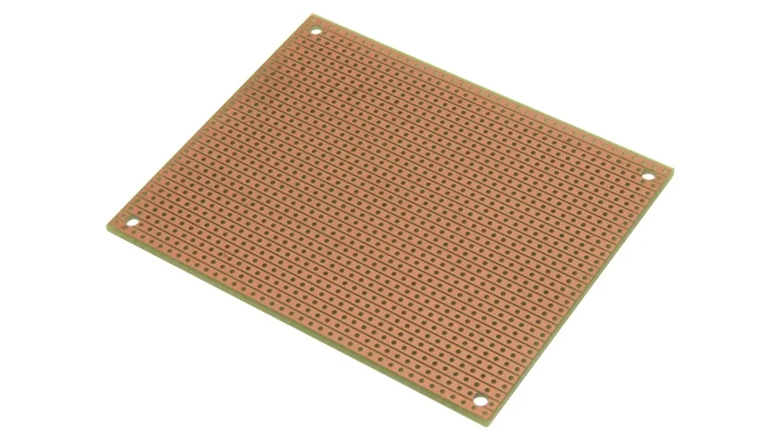
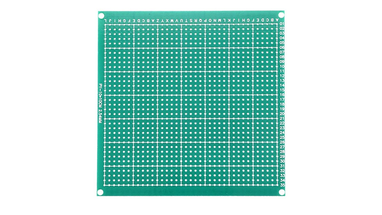
Zero PCB is a general-purpose circuit board specifically designed for prototyping and testing electronic circuits. Traditional printed circuit boards feature copper traces etched into predetermined layouts. Zero PCB adopts an entirely different design philosophy. Its substrate surface remains blank, with the primary structural characteristic being a regularly arranged matrix of pre-drilled holes. Each hole is surrounded by an independent copper pad. These pads are not interconnected by any predefined conductive pathways. This design grants users substantial creative freedom. Users can insert electronic components into corresponding holes and then freely connect the pads by manually soldering jumper wires or constructing solder bridges, thereby building complete custom circuits.
Features of Zero PCB
- Blank Canvas: Offers a blank canvas for users to create and test any prototype circuit.
- Grid of Pre-Drilled Holes: Holes arranged in a grid (typically spaced at 0.1 inches apart) fit most standard through-hole components.
- Surrounded by Copper Pad: Each hole is encircled by a copper pad, providing a reliable point for soldering.
- No Predefined Connections: Unlike custom or bare PCBs, there are no circuit traces or predefined circuit layouts.
- General-Purpose Design: Zero PCBs are usually made from FR-2 or FR-4 substrates, ensuring compatibility with a range of DIY electronics and custom circuit requirements.
Zero PCB Board Feature Summary
| Feature | Detail |
| Hole Grid | 0.1 inches (2.54mm) spacing |
| Copper Pad | Surrounds each hole; for soldering connections |
| Board Structure | Simple in structure to allow maximum flexibility |
| Layer Count | Single-layer (most common) |
| PCB Substrate | FR-4 (fiberglass), FR-2 (phenolic) |
| Applications | Prototyping, educational projects, small projects, repairs |
| Compatibility | Standard through-hole components (resistors, ICs, etc) |
Zero PCB Board Features, Structure & Design

The appeal of the zero PCB is its intentionally minimal structure. While a bare PCB (or custom PCB) has advanced features like multi-layer copper traces, solder mask and silkscreen for mass production, a zero PCB is made for flexibility:
- General-Purpose PCB: The structure allows for maximum customization—each user defines the electrical layout based on their project.
- Simple Structure: Lacks extra layers or specialized etch; the only copper is the thin pad surrounding each hole.
- Direct Component Insertion: You build a circuit by inserting components into these holes, then connecting pads using wires or solder.
- Adaptability: Need a new circuit design or want to update your existing prototype? Just cut traces, desolder and rearrange—zero PCBs are perfectly suited for design iteration.
- Customizable Layout: Users can build power buses, grouped grounds or any special function just by wiring under or over the board.
- Dot PCB: The zero PCB, also known as “dot PCB,” is functionally the same – emphasizing a versatile grid of conductive dots for any basic circuit design.
Benefits of Zero PCB Structure:
- Allows prototyping circuits without waiting for PCB fabrication
- Excellent for testing circuits prior to designing a custom PCB
- Great teaching aid for basic circuit design and soldering
Zero PCB vs Bare PCB: Understanding the Difference
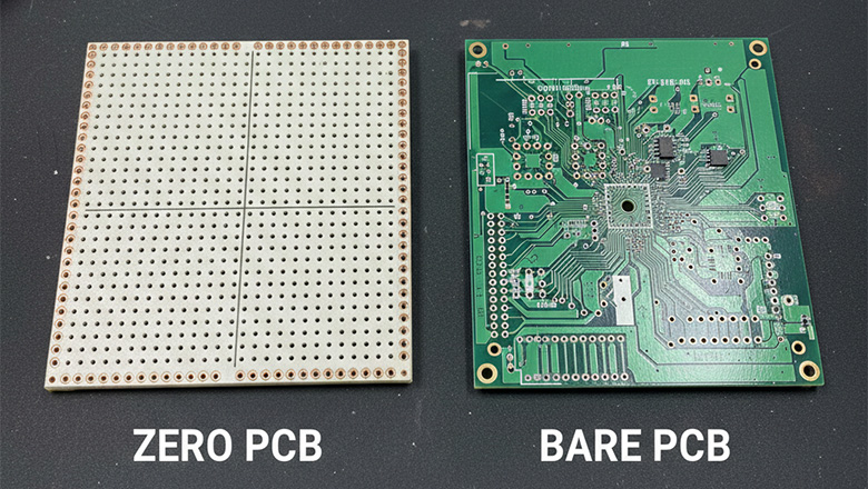
One of the most common questions for beginners and seasoned engineers alike is: zero PCB vs bare PCB—which should I use?
Bare PCB
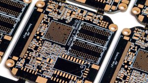
A bare PCB is a board that has undergone the manufacturing process (etching of copper traces, drilling, applying solder mask and silkscreen) according to a specific circuit design, but with no components yet assembled. It’s like an architect’s blueprint made real, but empty. Bare PCBs are the foundation for mass production, value consistency and scale.
Features of Bare PCB:
- Predefined circuit layout, copper traces and pads
- Often includes a solder mask and silkscreen for component labeling
- Designed for a single application, limiting further changes
- Intended for PCB assembly after complete design
Zero PCB
A zero PCB is intentionally left devoid of any etched copper traces or predefined layouts. Its only pattern is the regular grid of pre-drilled holes, surrounded by copper pads, offering endless possibilities for general-purpose circuitry.
Zero PCB vs Bare PCB Table
| Feature | Zero PCB (General-Purpose) | Bare PCB |
| Copper Traces | None (manual wiring needed) | Predefined by designer |
| Etching | Not required | Required (for circuit layout) |
| Design Requirements | None (blank canvas) | Must match specific project |
| Flexibility | Extremely high | Low after fabrication |
| Ideal Use | Prototyping, small projects | Mass production |
| Predefined connections | No | Yes |
Summary:
- Use a zero PCB when you want flexibility, iteration, and fast prototyping.
- Use a bare PCB for professionally-finished, mass-produced electronics.
Types of Circuit Boards for Prototyping

There is a range of general-purpose pcb types for creating and testing circuits. Understanding their benefits of zero pcb vs breadboard vs other boards will ensure you pick the right type for your electronics project.
1. Zero PCB Board (Perfboard/Dot PCB)
- Blank board with a grid of pre-drilled holes and copper pads
- Requires soldering to connect components
2. Breadboard
- Temporary solution for fast prototyping; push-in wire connections, no soldering needed
- Not durable or reliable for permanent builds
3. Stripboard (Veroboard)
- Copper traces run in parallel rows, simplifying bus or repeated connections
- Can be modified by cutting traces to match custom layout
4. Custom Printed Circuit Board (Printed Circuit Board/PCB)
- It is designed and manufactured to meet the highly specific technical specifications and functional requirements of the final product.
- Best for mass production or complex multi-layer circuits
Type of Circuit Board Comparison
| Board Type | Ease of Customization | Structure | Durability | Typical Use Case |
| Zero PCB | Maximum | Simple grid | High (soldered) | Prototyping, small runs |
| Breadboard | Very high | Spring contacts | Low | Early experiments |
| Bare PCB | None (predefined) | Etched traces | High | Mass production |
| Stripboard | High (rows/buses) | Parallel lines | High | Power/logical circuits |
How to Use a Zero PCB: Step-by-Step Guide
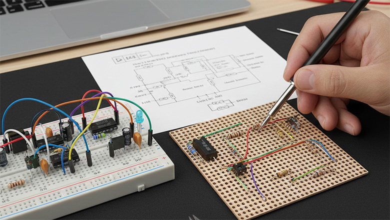
Building your own circuit board using a zero PCB board is a hands-on learning approach. This method enables designers to practice custom circuit design, test new ideas and prepare technically for subsequent mass production of printed circuit boards. This article will provide a step-by-step demonstration of how to create and test custom circuits with a zero PCB, covering the complete process from planning to debugging.
1. Designing Your Circuit Layout
Before you touch your soldering iron, sketch out your circuit layout. Remember, a zero PCB board is a blank canvas for users to create – the absence of a predefined circuit layout lets you be inventive. Consider:
- Which components you’ll use (e.g., resistors, capacitors, IC chips)
- How you’ll arrange them to keep wires short and reduce noise/interference
- Where connections (power rails, ground, in/out signals) will run for your prototype pcb
2. Inserting Components into the Holes
Take your components and begin inserting components into the holes of the zero PCB. The strong point of a board for your electronic prototyping is that the hole grid makes it easy to customize the build:
- Components like resistors and ICs fit neatly into the 0.1 inch grid spacing
- Group related components close together for tidy wiring
- Place larger items (connectors, switches) along board edges for easy access
3. Soldering and Wiring
Once you’re satisfied with your layout:
- Solder each component’s lead to the copper pad surrounding the hole.
- Connect components using insulated wires for long jumps or direct solder bridges for adjacent pads.
- For circuits requiring common power or ground, create “rails” by linking multiple pads together with bare wire or a soldered bus.
4. Testing and Iterating
After your circuit is soldered and wired up:
- Inspect for solder bridges or cold joints that could cause issues.
- Use a multimeter to verify key connections and check for shorts.
- Power up your circuit with an adjustable supply and look for functionality.
- If changes are needed, disconnect wires, desolder and rearrange as required – the benefits of zero pcb boards are their ability to be reworked without waiting for new PCBs!
Applications of Zero PCB
Zero PCBs are widely used due to their flexibility and low cost. Here are some popular applications of zero pcb:
- Prototyping for Engineers and Hobbyists: Quickly create and test custom circuits before committing to a full printed circuit board for mass production.
- Educational Purposes: Perfect for teaching students the basics of basic circuit design and soldering without the pressure of PCB manufacturing lead times.
- DIY Electronics: Makers and hobbyists use zero PCB boards for small projects, home automation, IoT gadgets and unique repairs.
- Quick Fixes: Repair or modify existing electronics with a board that will fit any situation – no waiting for custom etched boards or bare PCB delivery.
- Functional Testing: Build prototype circuits to test devices or subsystems and iterate easily, using your zero PCB as the perfect general-purpose prototyping board.
Advantages and Disadvantages of Zero PCB
Understanding the advantages and disadvantages of zero PCBs relative to other board options plays a key role in selecting the most suitable circuit design solution for your project. These options include bare boards, breadboards and custom printed circuit boards. Clarifying their respective characteristics and limitations forms the essential basis for making an informed decision.
Advantages of Zero PCB Boards
- Maximum Flexibility: The lack of predefined connections means you can create virtually any circuit on them by inserting and wiring components as you wish.
- Cost Effective: Much cheaper than ordering a custom printed circuit board for every prototype or small run.
- Easy to Iterate: Need to adjust your circuit? Just cut a wire, desolder and reconnect—zero PCBs offer easy revisions.
- Simple in Structure: The intentionally kept simple layout provides a canvas for users to experiment.
- Widely Used: Zero PCB is widely used for educational, hobby and professional purposes due to its utility and ease of use.
- Quick Turnaround: No delays for fabrication, shipping or ordering a new bare pcb when you want to test a new idea.
Disadvantages of Zero PCB Boards
- Labor Intensive: Complex circuits can become a tangle of wires and take longer to build than circuits on a predefined PCB.
- No Professional Appearance: Finished zero PCBs lack the polish and repeatability of a custom bare pcb or mass-produced board.
- Difficult for High-Frequency Circuits: Limited by the manual wiring; not suitable for high-speed, impedance-sensitive designs.
- Not Suited for Very Large Projects: For intricate or production-ready boards, a custom-designed printed circuit board is more efficient.
- Potential for Human Error: Manual wiring and soldering can lead to mistakes that are rare with etched copper traces on zero pcbs.
Tips for Creating High-Quality Circuits on a Zero PCB Board
To get the most out of your zero pcb board, follow these high-quality PCB assembly and design tips:
- Plan Ahead: Sketch your circuit layout and double-check compatibility with the hole grid. Efficient planning saves time and reduces wiring errors.
- Keep Wires Short: Short, direct connections improve performance and prevent electrical interference.
- Use Color-Coded Wiring: Helps to identify power, ground and signal paths.
- Inspect Solder Joints: Take time inspecting your soldered pads for shiny, smooth connections.
- Test Frequently: Use a multimeter to check each connection as you build.
- Reinforce for Durability: Use a dab of epoxy or hot glue on heavy components or connectors.
- Document Layouts: Write down modifications or jumper wire changes—a must for troubleshooting or teaching others.
FAQs About Zero PCB Boards
Q: What is the difference between a zero PCB and a bare PCB?
A: Zero PCB is a generic blank circuit board. Designers build circuits on it by manually routing wires and performing soldering. In contrast, a bare board is a circuit board specifically manufactured according to a predefined circuit layout. Its surface has been etched to form specific copper traces. This customized design makes it directly applicable for subsequent mass production.
Q: What are the main features of zero PCB?
A: The typical structural feature of a zero PCB is reflected in its regularly arranged matrix of pre-drilled holes on the surface. Each hole is equipped with an independent annular copper pad. This deliberately simplified physical structure provides designers with maximum design freedom. Based on this structure, designers can freely establish circuit connections and achieve rapid prototyping.
Q: When should I use a breadboard vs zero PCB?
A: Breadboards are suitable for scenarios that require quickly assembling prototypes and testing temporary circuits. When the design objective shifts to building more durable, long-term custom circuits, zero PCBs should be selected instead. Zero PCBs can provide secure soldered connections and support flexible, personalized design adjustments.
Q: What type of circuit board is best for educational projects?
A: Zero PCBs are widely adopted in educational settings. Their structural characteristics make them an ideal teaching aid, helping students understand fundamental circuit design principles while practicing hands-on soldering skills. These skills form a fundamental component of practical electronics competency.
Q: Are zero PCBs only for beginners?
A: No—engineers and professionals use zero PCBs for prototyping, testing and even as field-ready low-volume solutions.
Conclusion: Should You Use Zero PCB for Your Next Project?
The zero PCB is to offer a blank canvas for users to create and test any design requirement with unmatched customization. Its general-purpose nature and intentionally simple structure make it the go-to solution for engineers, students, hobbyists and anyone involved in basic circuit design and soldering. Whether you’re building small projects, educational kits or creating proof-of-concept prototypes, the benefits of zero PCB are clear: fast iteration, cost effectiveness, maximum flexibility and valuable hands-on experience with real electronic components. Zero PCBs are usually the first step from idea to reality for both DIY electronics hobbyists and professionals in research and development.
When should you choose zero PCB boards?
- When you require a customizable, general-purpose platform for circuit design and assembly.
- If you need to create and test custom circuits rapidly without waiting for a new bare PCB.
- When your project or educational goal emphasizes learning the principles of electrical connectivity, PCB layout and soldering basics.
- For prototyping unique circuits that don’t yet justify the time and cost of mass production via custom printed circuit boards.
When to consider other options:
- If your circuit is final, complex or needs to be manufactured in quantity, opt for a custom fabricated PCB board.
- For ultra-high-speed, high-frequency or surface mount designs where a tight PCB layout and well-controlled impedance are mandatory.
Ultimately, zero PCB offers an intentionally simple in structure yet powerful means to iterate, learn and innovate with electronics. So the next time you want to build a circuit from scratch, solve an urgent problem or teach the next generation of engineers, reach for the general-purpose zero PCB board—the most adaptable canvas for users to create and connect components however their imagination and requirements demand.