
Introduction
In the world of PCB design, precise component placement is at the core of every successful electronic device. Whether working with discrete resistors or BGA microcontrollers, the way components are placed on the pcb radically shapes manufacturability, functionality and long-term reliability. This comprehensive guide explores the basic PCB component placement guidelines every designer—amateur to expert—should understand. We’ll cover not only placement rules but also how PCB design tools can help create the best component placement for your project.
Why PCB Component Placement Guidelines Matter

Understanding why pcb component placement guidelines matter is step one toward superior design. Each component placement decision affects pcb assembly, test, signal quality and durability.
Proper component placement ensures:
- Clear routing for traces
- Better thermal management
- Reliable high-speed components operation
- Simplified pcb assembly
Strong immunity to component failure from stress, EMI or heat
Basic PCB Component Placement Guidelines: The Foundation

If you want to create the best component placement, guidelines for effective board layout and component positioning strategy are absolutely essential. These basic PCB component placement guidelines set the foundation for any robust PCB.
Key Principles
- Group Components by Function:Always organize components into functional blocks (power, digital, analog, RF, etc.)
- Position Components for Manufacturability:Place connectors and critical components near the edge of the board for easy access.
- Maintain Minimum Distances:Adhere to minimum distances of the components; components placed too close together may create shorts, assembly errors or component failure.
- Avoid Placing Tall Components Near the Edge:Place tall or heavy components at the center of the board or provide mechanical support.
- Thermal Management:Place components that generate heat away from sensitive components. Ensure room for airflow or heatsinks.
- Logical Flow:Arrange inputs, functional processing and outputs logically for easy routing.
- Avoid Placing Large Components Blocking Smaller Ones:Don’t let large connectors or power parts overshadow nearby passive components or block visual inspection.
Component placement guidelines will help everyone on your team—from circuit designers to assembly operators—work more efficiently, while also ensuring the design and manufacturing process runs smoothly.
General Rules for PCB Component Placement

Comprehensive Component Placement Rules
- Edge Clearance:Maintain manufacturer-recommended distance (typically 40–100 mil) for all components from the edge.
- Orientation:Standardize orientation of polarized and SMD components to aid automated pcb assembly and inspection.
- Board Space Optimization:Use both sides of the board if needed, but avoid placing sensitive or heavy components on the bottom unless necessary.
- Grouping:Group components such as power supplies, analog circuits, and digital logic into tight zones (“islands”) for simplified routing and fewer placement issues.
- Mechanical Support:Reinforce heavy or stress-prone components with vias, extra pads or standoffs.
- Component Markings:Ensure all component markings and polarity indicators are visible after assembly.
- Accessibility:Keep test points, jumpers and programming headers accessible, not trapped under large or soldered-in parts.
- Keep SMT and Thru-Hole Parts Organized:For mixed-technology boards, group SMT components on one side and thru-hole components on the other for efficient placement.
- Heatsinking:Plan copper pour and thermal vias around hot ICs, power inductors and FETs.
- Functional Separation:Isolate analog vs. digital vs. power regions to prevent signal interference—vital for high-speed components and sensitive components.
Organize components into functional zones. Position components logically. These rules for PCB layout help prevent common placement and routing headaches and ensure the rest of the placement is simple and reliable during both design and assembly.
PCB Component Placement Process: A Step-by-Step Approach

A professional pcb designer follows a set process when placing PCB components. Here’s an effective component placement strategy:
- Place Critical Components First:
- Connectors, battery holders, antennas at the side of the board or edges for accessibility.
- Components sensitive to noise, heat or vibration away from potential sources of interference.
- Group Supporting Components:
- Keep passive components(caps, resistors) near ICs using them (e.g., decoupling/bypass caps).
- Place bypass/decoupling caps as close as possible to VCC/GND pins.
- Place Active Components:Major functional ICs and subcircuits, centralized to minimize trace length.
- Fill with the Rest:Add remaining passives and non-critical discretes, observing minimum distances.
- Optimize Routing Paths:Review and nudge placements to optimize for clear, short routing paths and minimized via count.
Critical Placement Steps
| Placement Step | Component Types | Placement Tips |
| First—Edge I/O | Connectors, switches, LEDs | Place at true board edge, clear access |
| Second—Core ICs/Power | MPUs, regulators, amplifiers | Centralize, short path to decoupling |
| Third—Associated Passives | Bypass/decoupling caps, ferrites | Snug to their IC pins |
| Fourth—Remaining Discretes | Resistors, small diodes | Fill in unused board space, observe spacing |
| Fifth—Test/Debug Points | Headers, jumpers, test pads | Board edge is preferable |
Component Placement for High-Speed, SMT and Thru-Hole Components
Basic PCB component placement guidelines must be tailored for modern PCB technologies, such as high-speed, SMT components and traditional thru-hole components.
High-Speed Components
- Place high-speed components in close proximity for matched trace lengths and to minimize EMI.
- Avoid trace stubs and maintain signal integrity with controlled impedance and direct routing
- Sensitive analog parts (like ADCs) must be far from high-speed clocks and digital lines.
SMT Components
- Align SMD parts in the direction of the reflow conveyor to prevent tombstoning.
- Group SMD passives (0402/0603/0805) together for minimal pick-and-place head movement.
- For high-density SMT, avoid placing tall components next to smaller ones to prevent shadowing during pcb assembly.
Thru-Hole Components
- Place bulky, tall thru-hole components(transformers, connectors) away from small SMDs.
- Minimize the number of sides requiring THT; cost and assembly complexity grow when both sides are loaded.
Floor Planning: Functional Organization of PCB Components

Component placement requires clear functional zoning. Your placement of pcb components should reflect your schematic’s logical block diagram:
- Digital zone:CPUs, FPGAs, digital ICs, memory—central or near other digital parts.
- Analog zone:Sensitive op-amps, low-noise sensors—shielded and distant from noisy circuits.
- Power zone:All regulators, PMICs and power FETs together with attention to quick access for cooling and test.
- RF/Optical zone:Specialized, often at the edge for antenna/fiber connections.
Guidelines tailored to your product’s function mean that you’ll often balance electrical performance and physical accessibility. For instance, you may need to position components near the edge of the board for connectors or switch placement, even if the rest of the placement is dictated by signal integrity or shielding demands. Edge of the board features are critical for user interfaces, antenna placement and quick assembly. On the other hand, sensitive analog ICs and crystals are typically better off far from the edge and noisy components, tucked closer to the center of the board.
Effective placement also means that supporting components like decoupling capacitors, terminating resistors, or bias networks should always be grouped tightly with their active ICs. This helps you mitigate EMI, reduce the risk of component failure from incorrect returns, and streamline troubleshooting. This process supports optimal signal tracing and minimizes parasitic inductance.
Advanced Component Placement: Manufacturability & Assembly
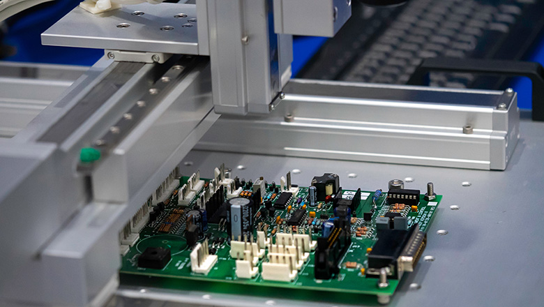
The component placement process isn’t only about performance; manufacturability is equally vital. DFM guidelines (Design for Manufacturability) ensure your board is easy and economical to produce.
Manufacturability Essentials
- Avoid components near the edge too closely to prevent handling, depaneling, or soldering issues.
- Place large components and fragile devices away from anticipated mechanical stress points.
- Use fiducial marks and tooling holes to aid automated placement equipment.
- Design for pick-and-place assembly by standardizing component orientation and minimizing part rotation.
- Position components for automated optical inspection, ensuring markings are visibleand avoid shadowing.
- For boards with SMT and thru-hole components, group all SMT on one side where possible and use the other for larger THT elements.
- Place test points, programming headers, and debug connectors in accessible locations to minimize assembly and field service overhead.
Component placement guidelines will help you reduce placement issues on the assembly line and maximize yield by minimizing misplacement, solder bridging and tombstoning.
Placement Issues and How to Optimize Board Space
Smart component placement rules help avoid classic design and manufacturing pitfalls and optimize board space.
Placement Issues to Avoid
- Components placed too close together: Results in solder bridging, inadequate heat dissipation, difficult test access.
- Components on the pcb edge or too near board outline: Increases the risk of shorts, mechanical damage or solder issues during depaneling.
- Failing to allow for rework/tools:Proper component placement requires leaving space for rework tools and test equipment.
- Unplanned routing congestion:Not leaving adequate space for high-pin-count BGAs or connectors can create dense areas with impossible-to-route signals.
How to Optimize
- Use both sides of the PCB for low-frequency, non-critical, or shielded components, but remember cost implications.
- Place high-value or sensitive nodes near the center of the board, optimizing light and airflow/heat sinking.
- Combine passive components into resistor/capacitor networks when possible, reducing individual placements and freeing up board space.
- Components near board edges should be reserved for UI, power connectors, and antennas as the only exceptions and should observe recommended minimum spacing.
- Placement and routing should always be validated together—don’t finalize position until you’ve traced critical nets and verified there are practical paths.
Modern PCB Design Tools: Optimizing Component Placement
Today’s PCB design tools can help you build better boards by automating checks, validating footprints and running design rule checks (DRC) in real-time.
How PCB Design Tools Can Help
- Automated constraint management: Most pro tools enforce minimum distances of the components, clearances, zone separation and other rules for PCB.
- Placement recommendations: Many platforms suggest optimal location for decoupling caps, high-speed lines and even group components automatically.
- 3D visualization: View your board in 3D, check mechanical collisions and ensure all connectors and large components are positioned to avoid placement issues.
- Simulation and analysis: Modern suites offer thermal, signal and power integrity analysis that highlight problem areas in real-time, enabling you to reorganize components before prototyping.
PCB design tools can help create the best component placement and drastically reduce errors that lead to expensive PCB re-spins or board failures.
Common Mistakes and Placement Issues to Avoid
Even the best designers make mistakes—but learning from these is how you establish robust placement rules and design habits.
Common Mistakes
- Neglecting edge clearance: Components placed too close to the edge can be damaged during cutting or handling.
- Overcrowding critical areas: Dense regions beneath BGAs can make inspection impossible and risk soldering defects.
- Ignoring thermal flow: Components that generate significant heat but are crammed together will create local hot spots and possible board failures.
- Failing to align components for assembly: Inconsistent orientation slows down both manual and automated placement, increasing costs and the risk of placement errors.
- Blocking test and debug access: Carefully consider future troubleshooting—accessible test points and clearly marked programming headers are a must.
Frequently Asked Questions
Q: How close should PCB components be placed to the board edge?
A: Always follow manufacturer recommendations—typically a minimum of 50mil, but often up to 100mil or more for high-voltage/connector areas. This prevents placement issues during board separation and enhances reliability.
Q: What if components are placed too close together?
A: This increases the risk of solder branching, limits airflow, complicates rework and leads to a higher failure rate. Minimum spacing rules are vital for manufacturability and inspection.
Q: Can PCB design tools really help with placement?
A: Absolutely. Modern EDA tools flag violations, offer placement/routing suggestions, let you analyze board space and even automate functional grouping. They’re indispensable for complex designs.
Q: Should passive components be grouped?
A: Yes—group passive components like decoupling and bypass capacitors close to their relevant ICs to reduce impedance and noise and optimize board space.
Q: Where should critical components be placed?
A: Place critical power, analog, or high-speed components in the central part of their functional block, away from heat sources or EMI/noise areas, to improve overall system stability.
Conclusion: Creating the Best Component Placement
In the world of PCB, component placement guidelines will help you not only build a board that works out of the box but also ensure manufacturability, easy debugging, thermal stability and long-term reliability. Basic PCB component placement guidelines form the backbone of effective placement—starting with functional block zoning, critical edge assignments, thermal/EMI consideration and future-proofing for assembly and service. Well-optimized, rule-driven placement ensures you get the most board space efficiency, durability and performance from your design.
Always leverage modern PCB design tools to enforce placement and routing rules, embrace regular peer reviews, and never underestimate the value of thoughtful, accessible and logical organization of your pcb components. These practices will help create the best component placement and ensure that your placement process supports both design quality and manufacturing success.
Building on these principles, every pcb designer can create layouts that deliver in the lab, on the production line and in the real world. Component placement rules, when followed, not only save time and money—they are the foundation of every great electronic product.