Introduction to PCB Files in the Electronics Industry
In the modern electronics industry, the success of every printed circuit board (PCB) project hinges on the clear, precise and accurate preparation of the right PCB files. From the earliest sketch in a computer-aided design (CAD system) to final fabrication, files are used at every stage to ensure the end product meets stringent requirements.
Unlike other documents, a PCB file set does much more than communicate a visual layout or schematic—it represents the living repository of manufacturing data and defines every trace, pad, drill, component location and net connecting components in the PCB. Each file format, whether it’s a Gerber file, assembly file, or PCB design file, plays a critical role in moving your idea through the multifaceted design and manufacturing process in the PCB industry.
With growing demands for HDI boards, high-speed signals or complex bare PCBs, choosing and preparing the right manufacturing files—helping you convert the PCB file into actionable instructions—is more critical than ever.
Why PCB Files and Manufacturing Files Matter in PCB Manufacturing
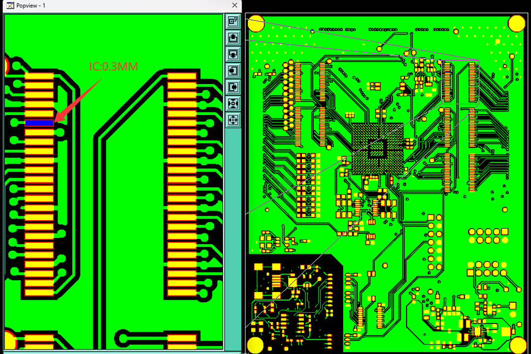
One file—if correctly prepared—can save weeks of expensive rework. But even a minor error can stall the entire PCB manufacturing or PCB fabrication process.
Why? Manufacturing files are not ordinary communication documents.These files serve as operational blueprints, which are interpreted by advanced automated equipment, plotters, CNC machines and inspection equipment.Various file formats work in coordination with each other to fulfill one shared task: building a bridge between the design and manufacturing processes that enables a seamless transition from the digital world to the physical world.
- PCB design files specify where each trace, pad or via is placed on the PCB board.
- Gerber files are responsible for format conversion.They convert the layout of the circuit design into a data format that can be read by photoplotters.The photoplotter then performs operations based on these data, separately creating images for each copper layer and each solder mask layer of the circuit board, and ultimately produces the films required for production.
- Associated NC drill files, BOM and assembly data tell factories exactly where to drill holes, place and solder electronic components or even test the finished assembly.
Without a robust suite of PCB manufacturing files, your board cannot be built—no matter how brilliant your circuit. This precision-focused workflow is the backbone not only of big brands but also of startups relying on turnkey manufacture and assembly. Accurate design documents ultimately guarantee both performance and manufacturability.
Types of PCB Files and Manufacturing Files: An Overview
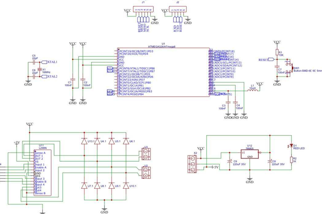
A typical design and manufacturing project produces a range of PCB files and manufacturing files, each with a distinct data format and purpose. Here’s an expanded look:
Core PCB Design Files
- Schematic Diagram: The netlist, logic and connections; often exported in a human-readable dxf format for sharing.
- Layout File: The physical representation, showing trace routes, layer stackup and actual component placement.
- Silkscreen Layer: Shows reference designators and graphics to aid physical manufacture and assembly.
- PCB Design Files: Any file from a CAD system necessary to regenerate, revise or analyze a board.
Key Manufacturing Files
| File Type | Format/Extension | Used For |
| Gerber Files | .gbr, .gtl, etc. | Imaging/plotting layers |
| NC Drill Files | .drl, .txt, .xln | Drilling data (holes, vias) |
| Bill of Materials (BOM) | .csv, .xls | Procurement, assembly, sourcing |
| Pick-and-Place Files | .csv, .txt | Machine coordinates for assembly |
| Paste Mask/Solder Paste | .gpb, .gtp, etc. | Stencil data for reflow soldering |
| Testpoint & Netlist Files (IPC-D-356) | .txt | Test automation and electrical checking |
| PDF Drawing | Human-readable assembly or fab instructions | |
| STEP/3D Models | .stp, .step | Mechanical integration |
Additional Files for Special Requirements
- Mechanical drawings (AutoCAD .dwg, .dxf formats)
- ODB++ files (consolidated data for advanced factories)
- Assembly files (detailed step-by-step build instructions)
From PCB Design to Fabrication: LHDPCB’S Design and Manufacturing Process

The entire process of a PCB project consists of multiple stages. The work of designers begins long before the circuit board goes into fabrication. Manufacturing equipment then transforms the design into a physical product. Finally, the product itself must undergo various tests, and the process concludes only after it has passed all certification judgments.
Stepwise Breakdown
- Schematic Capture: Engineers use PCB design software or EDA tools to create a logical diagram—connecting every net, part value and electrical connection.
- PCB Layout Creation: Engineers use PCB design software or EDA tools to undertake the task of drawing a logical schematic diagram. This schematic diagram contains every net node, each component value and all electrical connections.
- Output File Generation: Our designer exports the completed layout into several specific formats: Gerber files, NC drill files and other files required for manufacturing. These PCB fabrication files together form the most important data foundation and support for all subsequent manufacturing processes.
- DFM (Design for Manufacturability) Review: We perform an inspection task on the received PCB fabrication files. The purpose of this task is to identify whether there are errors, whether there are violations or whether there are any issues affecting manufacturability in the files.
- Manufacturing and Assembly: After approval, We proceeds with the production process. They fabricate the bare board according to the Gerber files, perform the drilling and manufacture all circuit layers. These steps are all aimed at preparing the board for the subsequent assembly.
- Assembly and Inspection: Machines and operators use assembly files, BOM and reference designators to place and solder each part. Inspection and test files (netlist, functional test) validate the assembled board.
The Gerber File: The Universal Language of PCB Manufacturing

Perhaps the most critical file format in the PCB industry is the Gerber file. The evolution from “aperture tables” to the integrated, metadata-rich RS-274X and Gerber X2 standards has allowed designers to include all information necessary for error-free plotting.
Gerber File Essentials
- What is a Gerber File? A Gerber file describes every graphical layer (copper, soldermask, silkscreen) as a machine-interpretable set of shapes, points and aperture commands.
- Gerber Format Standards:
- RS-274D: Legacy, requires separate aperture files.
- RS-274X/Gerber X2: Modern standards, supporting embedded pad info, file origin and layer designation.
- Widely adopted as the universal file format for all PCB manufacturers and plotters.
How Gerber Files Are Used:
- Plotters image copper, mask and silk directly from Gerber data. This ensures that “what you see is what gets built.”
- Factories in North America, Europe, and Asia all adopt the Gerber format, for the reason that it is a unified and reliable file format.
Deeper Dive: Common PCB Manufacturing Files and Their Formats
Common PCB manufacturing files include a variety of formats, each serving a specific role in supporting the manufacturing and assembly processes.Selecting the corresponding files correctly for different production steps is critical to the successful completion of PCB production and fabrication.
List of Common PCB Manufacturing Files
- Gerber Files: As described, these are the industry standard. Every shop requests the PCB Gerber files as the main manufacturing data set for image plotting.
- NC Drill File: Essential for via, mounting holes, press-fit connectors—contains X and Y coordinates for the CNC drill plotter.
- Bill of Materials (BOM): A table listing each component, value, reference designator and often procurement notes (manufacturer, distributor part number).
- Pick-and-Place Files: Specifies precise component locations (with X/Y coordinates and rotation), vital for surface-mount lines and robotic assembly.
- Assembly Files: Instructions on special requirements—like selective soldering, secondary operations, press-fit connectors, or wiring harnesses.
- Testpoint/Netlist Files: Used by test engineers; files such as IPC-D-356 support both post-assembly testing and network extraction in PCB design.
- Mechanical Drawings (often PDF Drawing or DXF format): Show board outline, cutouts, mounting holes and no-go zones.
- STEP/3D Files: For enclosure verification, thermal analysis and integration checks.
How LHDPCB’S Designers Generate and Verify Manufacturing Files

The PCB Design and Manufacturing Workflow
- Electronic Design: Begin with a schematic in a CAD system using advanced PCB design software—this design file forms the “brain” of every board.
- PCB Layout: Use the same or compatible pcb design software to define exact trace locations, component footprints, via positions and special requirements. The output is the layout file.
- Design Rule Check & File Export: Designers are required to perform DRC checks.The purpose of this inspection is to ensure the safety and manufacturability of the circuit board.Upon passing the check, the following types of files shall be generated:Gerber files, NC drill files, Bill of Materials (BOM), pick-and-place files, as well as all files required for test points and assembly.
- Output Verification: Open the exported pcb gerber files, drill, and paste layers in an independent Gerber viewer (e.g., CAM350 or Gerbv). Engineers will convert PCB documentation into all required file formats for the target factory.
- File Review & Distribution: Package all manufacturing data as a validated archive—a typical project might have a compressed ZIP file with 10–20 manufacturing files.
Editing, Converting and Opening PCB Files
Converting a pcb file between formats or platforms is common in the design industry, especially when teams use different CAD systems or when LHDPCB request an unfamiliar format.
Popular Scenarios
- Convert the PCB File from Eagle to Altium: Most tools allow import/export of design files, Gerbers, and even direct schematic and layout transfers.
- DXF to Gerber Conversion: Board outlines or mechanical layer info (drawn in mechanical design tools) is imported into a PCB CAD system, then exported as Gerber for universal use in fabrication.
- Opening and Editing Gerbers: Use CAM tools (CAM350, ViewMate or online viewers) to review each layer.
- Validating Drill Data: Upload your NC drill file and overlay it on copper Gerber files in a viewer. Holes should exactly match intended via/pad locations in the layout file.
LHDPCB’S Top Tips for PCB Design Files: Ensuring Reliable PCB Fabrication

Even veteran PCB designers follow checklists to ensure reliable data delivery. Here are essential tips:
PCB Design Tips
- Always use the latest PCB design software for compatibility and new manufacturing file format support.
- Name every manufacturing file clearly—avoid generic names like “file1.gbr.”
- Align all files to the same plotter origin (0,0) and consistent units (mm/inch)—this ensures CNC, assembly and all automation lines up.
Document all special requirements in your manufacturing files:
- Solder paste thickness and stencil cut for fine-pitch QFPs or BGAs.
- Press-fit operations, adhesive zones or underfill callouts.
- Conformal coating mask/keepout areas for harsh environments.
Double-check reference designators; mislabelled or missing reference designators can seriously impact assembly and inspection.
Review the Gerber file and NC drill in an independent viewer—never rely solely on your CAD system’s internal preview.
Preventing Errors: How to Check Manufacturing Data & Fabrication Data
Best Practices for Fabrication Data
- Overlay Checks: Load all Gerbers, especially copper and soldermask, together with NC drill data. Holes should line up perfectly with pads.
- Layer Count: Count number of Gerber files; missing a copper or mask layer is a very frequent error in multi-layer designs.
- Compare BOM and Layout: All components in the PCB should have a reference designator and a matching BOM entry.
- Validate Silkscreen Layer: Review text size and spacing. Ensure it doesn’t cover pads (which can cause DFM issues).
- Assembly Files Quality: If exporting pick-and-place or assembly files, make sure X and Y coordinates match the orientation and the same file origin as the layout.
Why Files To Ensure Quality Control?
- Design file consistency catches mismatches early.
- Manufacturing data reviewed independently helps engineers and production staff confirm intent.
- Fabrication data with fabrication notes (for soldermask, finish, etc.) reduces factory confusion and speeds up the quoting process.
Special Requirements and Advanced Aspects of the Design Industry
The world’s best PCB manufacturing projects go beyond just the basics. Here are advanced practices:
Incorporating Special Requirements
- For rigid-flex or HDI boards, specify stackup, controlled impedance layers and via-in-pad construction in supplementary files.
- For bare PCB delivered for assembly elsewhere, include board edge panelization, breakaway tabs and tool holes documentation in the manufacturing data.
- Use 3D/STEP files to check for inter-board assembly clashes in the mechanical enclosure at the design stage.
Assembly Files for Complex Manufacturing
- Special assembly files are used for instructions like partial population (not all BOM parts placed), applying underfill to specific components, or secondary soldering after the first reflow.
- When ordering turnkey assembly (full design and manufacturing), these extra documents help ensure there are no surprises for your contract assembler.
Conclusion and Further Resources
Conclusion: The Backbone of Reliable PCB Manufacturing
A robust PCB file set—carefully generated in standard file formats like Gerber, NC drill, and BOM—transforms bold electronic designs into high-quality physical products. In today’s electronics industry, efficient PCB manufacturing and assembly are impossible without precise, complete manufacturing files.
- Use modern PCB design software and stay current with file format updates.
- Document all special requirements and always check your manufacturing data in a third-party viewer.
- Remember: Only by ensuring every file is correctly formatted and complete can you achieve reliable, repeatable results in the highly competitive PCB industry.
Final Takeaways: Elevate Your PCB Design and Manufacturing Success
- Treat your PCB file and manufacturing files as mission-critical assets.
- Follow best practices for every design process—from layout to file export.
- Collaborate closely with our factories, using universal file formats to bridge design and manufacturing.
- Keep up-to-date with the latest in CAD software and file standards to ensure future proof workflows.