Printed circuit boards (PCBs) are the heart of almost all modern electronics, but not all of them operate under ideal conditions. Some have to withstand:
- Moisture and humidity
- Direct water exposure
- Constant vibration and mechanical shock
- Dust and airborne contaminants
- Chemical exposure in industrial settings
- Extreme temperature swings
A bare circuit board cannot last long in such situations. PCB potting gives that board a fighting chance. It seals the PCB inside a hardened component that shields it from moisture, vibration, dust, and chemical exposure.
This guide covers what PCB potting is, the materials behind it, the potting process, benefits, and its comparison with conformal coating. So, let’s jump right to it!
What is PCB Potting?
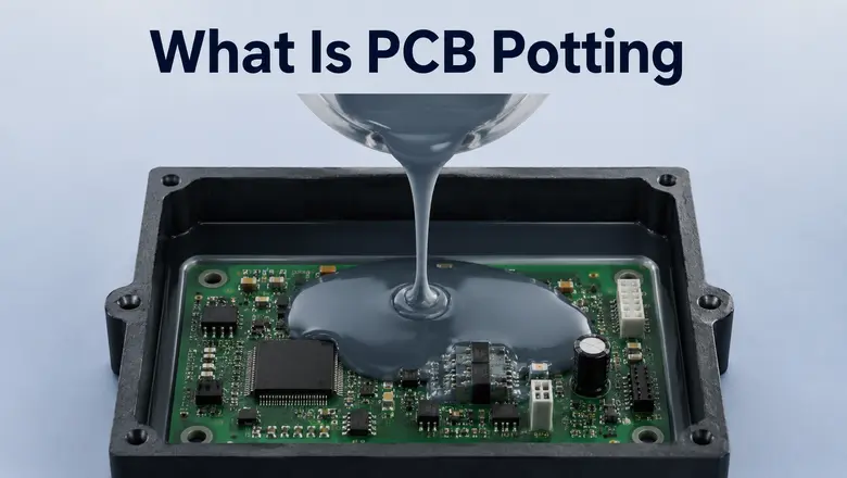
PCB potting is the process of encasing a complete electronic circuit board in a solid or gel-like electronic potting component. The material is usually made from epoxy, silicone, or polyurethane.
The purpose of PCB potting is to encapsulate the electronic components so they are fully shielded from external stressors, such as moisture, dust, chemicals, vibration, and physical impact.
During the process, the assembled board is placed inside a mold (called a “pot”) and then filled with the liquid component. As the material cures, it hardens into a solid protective layer that seals the board and everything mounted on it.
Potting and encapsulation are used interchangeably for this process, but there is a slight difference. Potting refers to filling a complete assembly within its enclosure, while encapsulation describes coating individual components in the board. However, the end result is the same in the form of a hardened protective layer that seals out the elements.
Why is PCB Potting Necessary?
Electronic devices are usually exposed to harsh working conditions that can degrade their performance rapidly. For example, an outdoor sensor module facing rain and humidity could short out without a sealed enclosure. Similarly, a board inside an automotive engine bay must survive extreme heat and chemical exposure from oil or fuel vapors.
PCB potting solves the above and many more problems at once, which is why it has been used as a go-to protection method for decades.
The following are some of the core reasons why PCB potting is necessary:
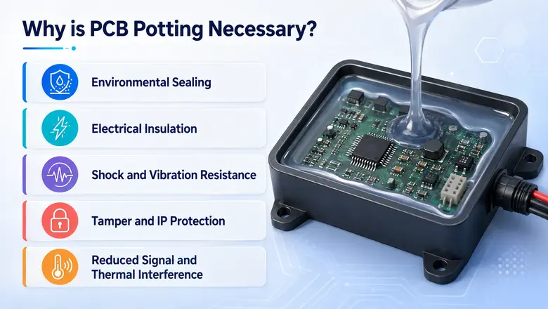
Environmental Sealing
A well-potted board gets strong protection against moisture, humidity, dust, and chemical penetration. This extends the working lifespan of the components inside.
Electrical Insulation
The potting compound also improves the board’s overall electrical insulation and reduces the risk of short circuits and electric shock.
Shock and Vibration Resistance
PCB potting provides mechanical support that helps absorb vibration and impact. This protects components from physical stress that would otherwise crack solder joints or dislodge parts over time.
When this is left unaddressed, the vibration from the board and its enclosure can actually couple together and amplify stress on the printed circuit board (PCB), which leads to premature failure.
Tamper and IP Protection
PCB potting has also found use outside pure environmental protection. It can serve as a deterrent against reverse engineering and help safeguard sensitive components such as cryptographic processing cards.
Reduced Signal and Thermal Interference
When dust and dirt are sealed out, potting also helps prevent buildup that can lead to overheating and signal interference.
Common PCB Potting Materials
It is important to choose the right potting material based on the level of protection you are trying to provide. The three common PCB potting materials in the market are:
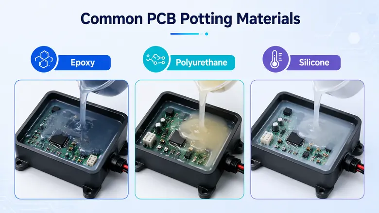
Epoxy
Epoxy is a common potting material, known for excellent mechanical strength and adhesion. It is suited for outdoor applications due to high rigidity and tensile strength. However, its main drawback is long curing time.
Polyurethane
Polyurethane is softer and more pliable. It is useful for protecting sensitive connectors and components that can’t tolerate a rigid material. It handles impact well and resists abrasion, but its moisture and heat resistance falls short of some alternatives. So, it is not the best choice for consistent humid environments.
Silicone
Silicone is a durable and flexible potting compound useful for applications requiring vibration damping or thermal expansion. It handles a wide temperature range (usually -60°C to 200°C) and provides solid protection from moisture spray.
How the PCB Potting Process Works
The PCB potting process involves a series of consistent steps to ensure complete coverage without causing any damage to electronic components. The step-by-step potting process is as follows:
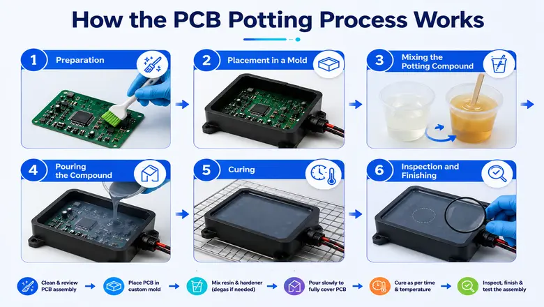
- Preparation: The PCB assembly is cleaned to remove dust and other contaminants that could affect adhesion. The component placement is also reviewed.
- Placement in a Mold: The PCB is placed in the custom mold (or “pot”) to hold the liquid compound. This shell can act as a temporary mold or the final housing.
- Mixing the Potting Compound: The resin and hardener are mixed according to the manufacturer’s recommended ratio. The mixture is stirred slowly to minimize air bubbles, and vacuum degassing may be used when necessary.
- Pouring the Compound: The potting compound is slowly poured into the mold from one corner. It flows around the components until the PCB is fully covered and all gaps are filled.
- Curing: The potted PCB is left undisturbed to cure for the time and temperature specified by the compound manufacturer. The curing process allows the liquid material to harden and form a protective layer.
- Inspection and Finishing: After curing, the assembly is inspected for bubbles, cracks, gaps, or incomplete coverage. Any excess material is removed, and electrical tests are performed to confirm that the PCB is functioning properly.
PCB Potting vs. Conformal Coating
In addition to PCB potting, conformal coating is another major option for protecting the board.
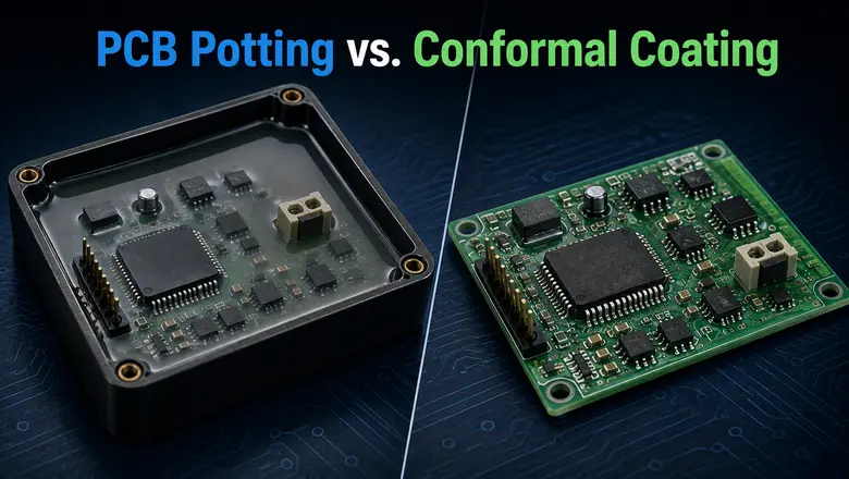
A conformal coating runs just 25 to 250 microns thick, which is a far lighter and more compact option than potting. Usually, this coating is applied as a thin layer by hand brushing/spraying or dip coating. It offers protection against humidity, dust, heat, and general corrosive exposure. Due to the thin layer, it keeps components accessible for repair.
PCB potting offers a much higher level of protection. It creates a fully sealed enclosure and provides greater resistance due to a thicker coating. Plus, it offers no realistic path to rework or repair once the board is sealed.
| Aspect | PCB Potting | Conformal Coating |
| Coverage | Full encapsulation | Thin surface layer |
| Thickness | Several mm | 25-250 microns |
| Weight | Heavier | Lightweight |
| Moisture Resistance | Excellent | Good |
| Vibration/Shock Resistance | Excellent | Moderate |
| Rework/Repair of Components | Not possible | Possible |
| Cost | Higher | Lower |
The general rule is that potting suits heavy-duty applications and high-voltage devices operating in extreme conditions. In contrast, conformal coating is useful for handheld electronics where size and weight are tightly constrained.
Applications of PCB Potting
PCB potting provides thorough protection, so it shows up wherever electronics are expected to withstand harsh conditions. The common applications of PCB potting include:
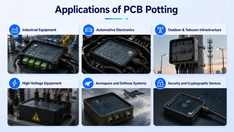
- Industrial Equipment: Control systems and power modules exposed to dust/chemicals and constant vibration on factory floors.
- Automotive Electronics: Components under the hood or in harsh underbody locations, where heat and moisture are a given.
- Outdoor & Telecom Infrastructure: Devices mounted outside that need to withstand weather year-round, such as street lighting controllers, base-station hardware, etc.
- High-Voltage Equipment: Transformers and switches, where potting helps prevent corona discharge and electrical arcing.
- Aerospace and Defense Systems: Applications demanding maximum reliability, where component failure isn’t an option.
- Security and Cryptographic Devices: Hardware that benefits from potting’s added resistance to tampering and reverse engineering.
Bottom Line
PCB potting isn’t required for every electronic product, but it becomes essential for those operating in harsh environments to ensure years of reliable use. However, it requires choosing the right compound and implementing the correct process. Working with a trusted PCB potting service like LHD Tech takes the guesswork out of material choice and process control, so your product performs reliably wherever it’s deployed.