
Introduction
In our hyper-connected world, circuit boards—the silent giants behind technology—carry electronic signals and power controlling smartphones, vehicles, computers, and industrial systems. At the heart of every device lies a thoughtfully architected circuit board pattern, turning abstract circuit design ideas into high-performance, robust realities.
This guide to circuit board patterns unveils the intricate world of PCB geometry, from the classic single-sided template to advanced multilayer PCB assemblies for digital circuits and wireless communication. We explore the essential nature of the network of conductive traces, geometric shapes, and pattern vectors—including how to leverage pattern design for optimal signal integrity, electromagnetic compatibility, and efficient power distribution.
You’ll discover why adherence to pcb pattern design guidelines and meticulous component placement determines the difference between ordinary and world-class electronics. Whether you’re a beginner learning about circuit patterns or a pro tackling high-density circuit requirements, this comprehensive guide arms you with design insights, practical checklists, and cutting-edge industry practices.
What is a Circuit Board Pattern?

A circuit board pattern refers to the circuit structure comprising the pathways and pattern vectors that direct the transmission of electrical signals across the board. It is the physical manifestation of a circuit design, translated into conductive traces, pads, vias, planes, pours, and sometimes even seamless graphic motifs reminiscent of seamless circuit board pattern wallpaper, which is popular in PCB artwork.
In engineering, this pattern is the core logic of any printed circuit board—defining how various components on the PCB connect for correct function. The circuit board pattern design includes intricate pattern vectors that map where each wire, pad, and via should go, ensuring every electrical connection required by the schematic is represented in copper.
There are always several layers of the circuit board:
- The top copper layer, usually bearing the most component density and critical signals.
- One or more inner layers(in a multilayer PCB) holding power planes, ground planes, or additional signal routes.
- The bottom layer, often reserved for less critical traces and connector pads.
A key distinction: A circuit board pattern is focused on the logical and electrical path, while the PCB footprint is focused on the geometry required for mounting components. Both must be perfectly aligned for a reliable finished product.
Importance and Function of Circuit Board Patterns

Circuit boards appear simple, but every circuit board pattern serves multiple, critical functions for practical and high-performance electronics:
- Network of Conductive Traces: These form pathways for electrical signals, linking chips, connectors, and passives. Correct network design minimizes noise and loss.
- Power Distribution: Well-designed power and ground planes, as well as broad traces, guarantee stable power supply to all devices and minimize signal attenuation and interference.
- Signal Integrity: Proper pattern design maintains controlled impedance and ensures signals, including high-speed digital signals, arrive undistorted and on time.
- Thermal Management: A good circuit board pattern enhances heat dissipation by using copper pours, power planes, and thermal vias to draw heat from power devices.
- Electromagnetic Interference and Compatibility: Maintaining solid ground planes and careful trace separation ensures “quiet” operation, especially in networking and telecommunications systems.
- Mechanical Support: The geometry of the pattern ensures all traces and components are secure, minimizing stress and board warping during assembly, testing, and real-world operation.
Key Insights
- A single design mistake—like an open trace or an unconnected pad—can compromise the entire board, causing re-spins, increased PCB manufacturing costs, and failed compliance testing.
- Best practice for power distribution is to use thick traces and solid planes, connecting decoupling capacitors close to integrated circuit power pins.
- Modern, high-density circuit requirements demand pattern vectors that are both compact and highly optimized for signal routing and switching.
Essential Functions and Roles of PCB Patterns
A PCB’s pattern is far more than random artwork on a board. Here’s why every detail matters for circuit performance:
- Provide Clear Pathways for Electrical Signals: Ensures reliable signal routing between logical blocks and minimizes signal reflections and crosstalk.
- Enable Power Distribution Through Planes and Traces: Solid power planes deliver current with negligible voltage drop; continuous ground planes ensure quiet returns for analog and digital blocks.
- Support Good Component Placement: By considering optimal vector routes for signals and power, circuit pattern enables tight placement without risking unintended shorts or interference.
- Aid in Electromagnetic Interference Suppression: Pattern design that avoids long open loops and keeps signals close to ground reference reduces EMI pickup/emission.
- Facilitate Testability and Manufacturability: Good patterning leaves space for test points and respects minimum trace width/spacing for pcb manufacturing.
Circuit Board Pattern vs. Footprint: Understanding the Differences
- The circuit board pattern refers to the network of conductive traces and components that make up the logical pathways of the circuit.
- The PCB footprint concerns the physical locations and pad geometries for components—the layout that ensures correct soldering, orientation, and spacing for assembly.
- Successful designs require matching the pattern to the correct footprints; otherwise, you risk assembly problems, intermittent/failed connections, or solder bridging.
Comparison Table:
| Feature | Circuit Board Pattern | PCB Footprint |
| Focus | Electrical connection, circuit routing | Mechanical placement, pad geometry |
| Role in Assembly | Determines trace/plane layout | Determines where and how to solder |
| Affects | Signal integrity, EMI, power distribution | Soldering quality, assembly time |
| Error Consequence | Non-functional/unstable circuit | Misaligned, unsoldered, or shorted part |
| Optimization | Minimizes noise and maximizes signal performance | Maximizes assembly and rework success |
Types of Circuit Board Patterns

Every project comes with its optimal geometry. Here are the types of circuit board patterns:
- Single-sided patterns: All traces on one side; used in simple/low-cost applications like calculators or remote controls.
- Double-sided patterns: Traces on both sides, often interconnected with vias; enables more complex circuits in compact footprints.
- Multilayer PCB patterns: Multiple layers of routed signals, power distribution planes, and shielding. Essential for modern complex circuits, servers, laptops, and advanced telecom gear.
- Power plane patterns: Broad copper regions dedicated to distributing high current efficiently; common in industrial controls and power supplies.
- Ground plane patterns: Large ground references reduce EMI and guarantee a quiet signal return. Especially critical for analog, RF, and digital systems.
- Differential pair routing patterns: Carefully matched length/width traces for pairs carrying complementary signals—vital in USB, HDMI, Ethernet, and other high-speed standards.
- RF transmission line patterns: Controlled-impedance microstrip or stripline geometries enable gigahertz and wireless communication with precision.
- Clock distribution patterns: Carefully orchestrated “clock tree” or star layouts to avoid skew and jitter.
- Seamless circuit board pattern: Used decoratively and, in some RF/EMI applications, for uniform field distribution or aesthetic PCB backgrounds.
- Pattern vectors and circuit board pattern vectors: Refers to both the directional flow of signals and to graphical vector resources used for creating or visualizing highly detailed board patterns, helpful in design presentations or educational materials.
PCB Pattern Design Guidelines and Considerations
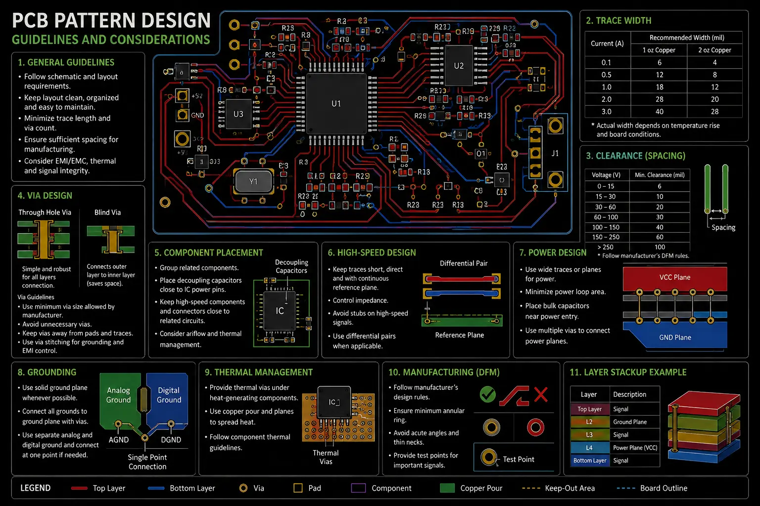
Meeting modern design challenges means applying solid pcb pattern design guidelines from concept to manufacturing:
Adherence to Design Rules
- Always follow your manufacturer’s minimum trace width, spacing, and via diameter. Violation leads to defective boards or low production yield.
- Remember that different layers may have slightly different constraints based on the mechanical properties of the materials and fabrication technique.
Component Placement Tips
- Place heavy or high-pin-count components first, ensuring sufficient space for other devices and future rework.
- Traces and components with sensitive or high-frequency signals should be kept short and direct—this reduces noise coupling and interference.
Power Distribution and Grounding
- Use simultaneous power plane and ground plane layers for optimal separation of signals and power, reducing chance for signal attenuation and interference.
- For high-current paths, employ polygon pours or wide copper traces, leveraging the entire board width when possible.
Controlled Impedance and Signal Integrity
- Calculate trace width and stackup distances for critical nets, especially those involved in differential pair routing or high-speed digital circuits.
- Route differential pairs together and match their lengths for minimized skew—a must in USB, HDMI, and high-speed memory layouts.
Thermal Management and Heat Dissipation
- Employ thermal vias under heat-generating chips, especially in LED, power supply, and motor controller boards.
- Connect copper pours and planes to all available pads for more efficient heat dissipation.
- Use simulation tools to assess hot spots and re-route for improved airflow or heatsink efficiency.
Electromagnetic Interference (EMI) and Electromagnetic Compatibility (EMC)
- Avoid running parallel high-speed or high-current traces to minimize signal reflections and crosstalk.
- Solid ground planes help contain stray fields and shield sensitive circuitry, making compliance with electromagnetic compatibility(EMC) easier.
- Where possible, use geometric shapes in copper pours for enhanced shielding effects.
Signal Routing and Switching
- Route high-priority or clock signals first, then critical data, followed by less sensitive lines.
- Minimize the number of vias—each via adds series inductance, which can degrade high-speed signals.
Advanced Topics: PCB Patterns in Telecommunications and Networking
Within telecommunications and networking applications, the circuit board pattern must meet demands of speed, reliability, and scale. Network equipment like routers, switches, and 5G transceivers use advanced multilayer PCB designs with dozens of different layers, each supporting a specific function.
High-Speed Signal Integrity
- Successful circuit performance in telecom requires precise length-matching, tight impedance control, and rigorous EMI shielding in the pattern.
- Networking systems benefit from star or tree-style clock distribution and careful isolation of high-speed nets.
Signal Routing and Switching in Networking Systems
- Large-scale network nodes deploy hierarchical signal routing and switching using a network of pattern vectors across circuit boards.
- Key signals are routed in parallel planes for distributed backplanes, minimizing latency, and protecting signal integrity.
Wireless Communication and RF Patterns
- Signal attenuation and interference are major challenges. RF paths are carefully routed with geometric shapes and controlled-impedance structures to minimize loss.
- PCB antennas require specialized seamless patterns, often with specific pattern vectors for directional gain.
Design Process: How to Create and Optimize a Reliable Circuit Board
Step 1: Schematic and Netlist Creation
- Use a vector-based schematic editor to ensure every electrical connection and signal net is accounted for.
- Simulate at this stage for early detection of design errors.
Step 2: Component Placement
- Place connectors and power devices along board edges for cooling and ease of assembly.
- Arrange digital and analog blocks to minimize parasitic coupling—this division aids thermal management and signal integrity.
Step 3: Routing Strategy
- Start with power and ground planes, then move to clock, data buses, RF, and less critical signals.
- When working across layers of the circuit board, always provide clear via paths and minimal trace length for maximum circuit performance.
Step 4: Simulation and Prototyping
- For complex circuits or those with high-speed content, simulate for signal integrity, voltage drop, and heat dissipation.
- Build and test a prototype using DFM (Design for Manufacturability) rules, then iterate based on real measurements.
Manufacturing Constraints and Real-World Tips
Key Manufacturing Considerations
- Respect minimum trace width and spacing to boost yield and reduce open/short circuits—typical values are 4–6 mil (0.10–0.15 mm).
- Panelize smaller PCBs to reduce handling costs.
- Choose insulating materials that suit your frequency; FR-4 is suitable for most circuits, while PTFE-based materials are essential for high-frequency wireless or radar systems.
Solder Considerations
- Use the correct pad geometry for reliable solder joints, especially for surface-mount devices.
- Clean board surfaces after assembly to avoid conductive residue or flux bridges, both of which can degrade signal integrity and cause corrosion.
Pattern Design for Assembly
- Include fiducial markers and test pads for automated assembly and QA.
- Silkscreen clearances and legend labels should not obscure pads or vias—clear visual indication streamlines assembly and repair.
PCB Pattern Troubleshooting: Common Problems and Solutions
Problem: Unstable digital signals Cause: Signal traces too long, lack of ground plane Solution: Shorten traces, add a continuous ground reference for improved EMI suppression.
Problem: Poor heat dissipation Cause: Skinny supply traces under high current, few or no thermal vias Solution: Use thicker power traces, increase copper pour area, and deploy thermal reliefs.
Problem: Faulty component placement Cause: Inadequate spacing for large or odd-shaped packages Solution: Use vector templates for footprints, verify with 3D PCB viewers, and consult component datasheets.
Problem: Excessive noise coupling and interference Cause: Parallel analog and digital lines, lack of shielding Solution: Separate analog/digital domains, use ground pours and keep analog traces away from digital switching lines.
Tools and Resources for Circuit Board Pattern Design
- EDA Tools: Altium Designer, KiCAD, Eagle, OrCAD—these enable detailed pcb design with robust vector editors.
- Simulation: HyperLynx, ANSYS SIwave for signal integrity, and thermal simulators for heat flow.
- PCB Libraries: SnapEDA, UltraLibrarian for verified footprints and schematic symbols.
Conclusion
In the evolving landscape of electronics, the circuit truly begins with the blueprint of a well-crafted circuit board pattern. From effective signal routing and power distribution, to robust thermal management and reliable solder connections, the entire design process determines the outcome. By mastering different layers, using correct pattern vectors, and respecting both pattern design rules and physical constraints, any engineer can produce a reliable circuit board ready for fabrication and world-class applications.
Remember: Always start your PCB pattern design with careful planning, learn from field failures, By focusing on design upfront, leveraging simulation and validation, and maintaining close communication with your PCB manufacturing partners, even the most complex circuits can be transformed into reliable, cost-effective, and innovative products. Whether your goal is to minimize electromagnetic interference in a sensitive RF module, optimize signal routing in a high-speed networking systems backplane, or streamline component placement for mass production, the fundamental principles remain the same: meticulous planning, adherence to pcb pattern design guidelines, and respect for the realities of manufacturability.
The future of electronics innovation lies in the mastery of the vector-driven art of the circuit board pattern. As advances push toward even denser, more interconnected designs in automotive, industrial, and wireless communication sectors, your ability to create seamless circuit board patterns, manage different layers efficiently, and preserve both signal integrity and power distribution will continue to be decisive factors in determining success.
FAQ for “Circuit Board Patterns”
1. What are circuit board patterns?
Circuit board patterns are the conductive traces, pads, vias, and copper areas formed on a PCB. They create the electrical connections between components according to the circuit design.
2. How do I design my own circuit board?
Start with a circuit schematic, assign component footprints, place the components, route the copper traces, and define the board layers. The final layout should then be checked with DRC before generating Gerber files.
3. What is the recommended PCB layout?
A good PCB layout uses short signal paths, proper component spacing, continuous ground planes, suitable trace widths, and clear separation between sensitive, high-current, and noisy circuits.
4. What is the 3W rule in PCB layout?
The 3W rule recommends keeping adjacent PCB traces at least three trace widths apart where practical. This helps reduce electromagnetic coupling and crosstalk between signals.
5. How do I design a PCB layout?
PCB layout typically involves defining the board outline, placing critical components first, routing power and high-speed signals, adding ground planes, and completing the remaining signal traces before running design-rule checks.
6. How do you read a PCB layout?
A PCB layout can be read by identifying components, copper traces, pads, vias, ground planes, and layer information. Reference designators and the schematic help show how each physical pattern relates to the electrical circuit.
7. What are the basics of PCB design?
The basics include schematic design, component placement, trace routing, layer planning, grounding, power distribution, impedance considerations, and manufacturing design rules.
8. What are the basic PCB design guidelines for beginners?
Keep traces short, use appropriate trace widths and spacing, place decoupling capacitors close to IC power pins, maintain a solid ground path, and always follow the PCB manufacturer’s design capabilities.
9. How do you identify PCB layers?
PCB layers are identified through the layer stackup and fabrication files. Common layers include top and bottom copper, internal signal layers, power or ground planes, solder mask, and silkscreen.
10. Why do PCB boards fail?
PCB failures can result from poor trace design, insufficient spacing, thermal stress, manufacturing defects, contamination, component problems, or inadequate solder joints. Good PCB pattern design and manufacturing controls help reduce these risks.