Introduction
PCB (Printed Circuit Board) is an integral part of building almost all modern electronic devices. It serves as the backbone that connects components electrically and holds them physically in place. It packs everything into a footprint small enough to fit inside the final product.
PCB circuit boards give devices shape and capability that enable semiconductors inside to exchange data at the speed modern electronics demand. Every smartphone, laptop, and piece of factory electronic machinery relies on a PCB underneath to function.
This guide walks through what a PCB (Printed Circuit Board) is, its components, working principle, types, manufacturing, and more. Stick around and learn why it has become such a foundational part of the technology we rely on every day.
What is a PCB Printed Circuit Board?
A Printed Circuit Board (PCB) is a flat panel made from fiberglass or a similar insulating material with a network of copper traces running across (or through) it.
Those copper pathways carry electrical signals between components like resistors, capacitors, transistors, and ICs, all of which get mounted directly onto the board’s surface. It’s like the wiring system of an electronic device, just flattened and etched into a board instead of run through loose cables.
The board also acts as the physical skeleton that holds every component in place. This makes the whole assembly slot neatly into a device’s housing.
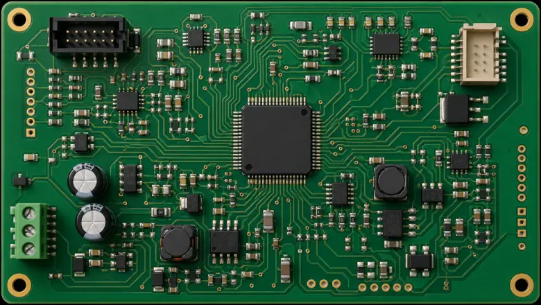
The important thing is that not every PCB circuit board is built the same way. Simple designs might only need a single layer of copper. However, more complex circuits call for double-sided or multi-layer boards, which stack several conductive layers on top of each other separated by insulation. Getting there involves etching away unwanted copper from each layer until only the intended trace pattern remains, then bonding those individual layers together under heat and pressure to form one solid stack.
Main Components of a PCB
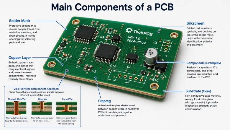
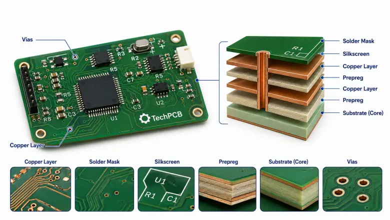
Every PCB (Printed Circuit Board) is built from a few crucial core layers, where each has its own job in making the final board work as intended. They all turn a flat piece of fiberglass into a fully functional platform for mounting and connecting electronic parts.
Substrate (Core)
The substrate is mostly a non-conductive rigid base of a PCB. It’s usually made from FR-4, a fiberglass fabric soaked in epoxy resin. This non-conductive material is chosen for its strength and heat resistance. This layer gives the board its physical shape and durability. It holds all the other layers together and keeps electrical signals from leaking where they shouldn’t.
Copper Layer
The copper layer sits on top of (or between) the substrate layers. It is where the actual electrical pathways live. It’s etched into traces/pads and larger copper pours that carry signals and power between components. There can be several copper layers in multi-layer PCBs. The copper thickness is usually 35 or 70 microns and varies for different current ratings.
Solder Mask
The solder mask is that familiar green (or sometimes red, black, blue) coating layered over the copper. Its main job is protection. It shields traces from oxidation, moisture, and accidental short circuits during assembly. It leaves exposed openings wherever a component needs to be soldered down.
Silkscreen
The silkscreen layer in a PCB circuit board adds the text, numbers, symbols, and outlines you see on a finished board. It is printed directly on top of the solder mask. It includes component labels, polarity markers, logos, and reference numbers. It doesn’t affect how the board functions, but it makes assembly/testing and troubleshooting far easier for humans.
Prepreg
Prepreg is the adhesive fiberglass sheet used to bond multiple layers together in multilayer boards. It sits between copper layers and fuses everything into a single solid stack once cured under heat and pressure. It acts as the glue holding a multilayer PCB together.
Vias
Vias (Vertical Interconnect Accesses) are the small plated holes that create electrical connections between different layers of the board. They let signals travel vertically through the stack, which makes multilayer routing possible in the first place.
How Does a PCB Work? A Step-by-Step Breakdown
A PCB (Printed Circuit Board) job is to give electricity a clear and organized path to follow. It connects the power, signals, and components in the exact sequence a circuit needs.
The workflow of a PCB involves these steps:
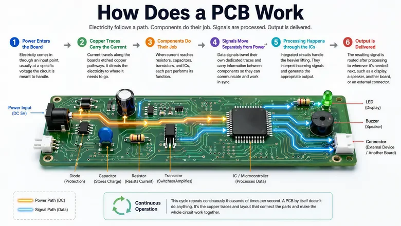
- Power Enters the Board: Electricity comes in through an input point, usually at a specific voltage the circuit is meant to handle.
- Copper Traces Carry the Current: Current travels along the board’s etched copper pathways. It directs the electricity to where it needs to go.
- Components Do Their Job Along the Way: When current reaches resistors, capacitors, transistors, and ICs, each part performs its function. It can be resisting current, storing charge, switching signals, or processing data. All this depends on what the circuit calls for.
- Signals Move Separately from Power: Data signals travel their own dedicated traces and carry information between components so they can communicate and work in sync.
- Processing Happens through the ICs: Integrated circuits handle the heavier lifting. They interpret incoming signals and generate the appropriate output based on the device’s programming or logic.
- Output is Delivered: The resulting signal is routed after processing to wherever it’s needed next, such as a display, a speaker, another board, or an external connector.
This completes the circuit’s task. The entire process happens continuously thousands of times per second. Overall, a PCB by itself doesn’t do anything. It’s the copper traces and layout that connect the parts and make the whole circuit work together.
Types of PCB Circuit Boards
There are several types of Printed Circuit Boards (PCBs) to fulfill various functional and design requirements:
-
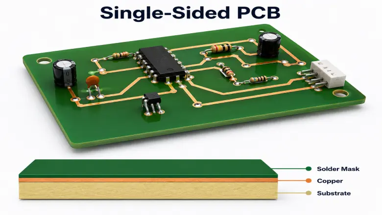
Single-Sided PCB
The simplest form of PCB in which copper traces run along just one side of the substrate. It’s cheap to produce and easy to assemble. It is a common choice for basic and low-density circuits, such as calculators, printers, radios, cameras, etc.
-
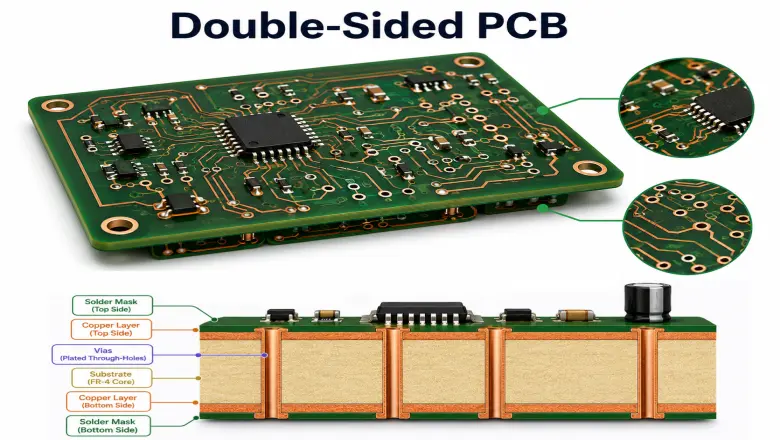
Double-Sided PCB
Copper layers exist on both sides of the board, with plated through-holes connecting the two. This doubles the available routing space compared to a single-sided design and allows configuration of more complex circuits. These PCBs are used in applications that require middle-level circuit complexity, such as HVAC systems, automotive dashboards, industrial controls, etc.
-
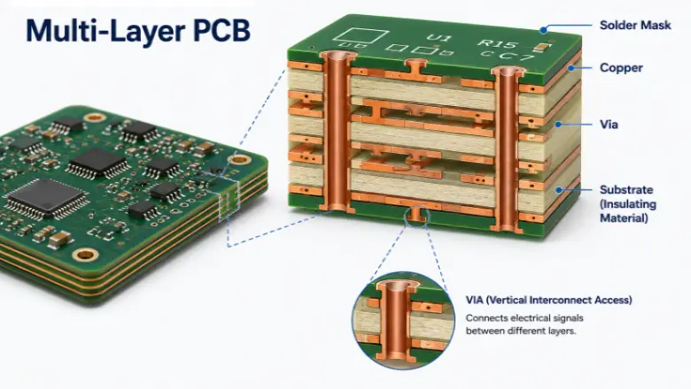
Multi-Layer PCB
Multi-layer PCB circuit boards stack three or more conductive layers together, separated by insulating material and bonded under heat and pressure. This construction supports much denser routing and higher component counts, which is why it’s the standard for compact and high-performance devices, such as smartphones, computers, satellite systems, etc. However, multi-layer PCBs require higher manufacturing precision to avoid alignment or lamination defects.
-
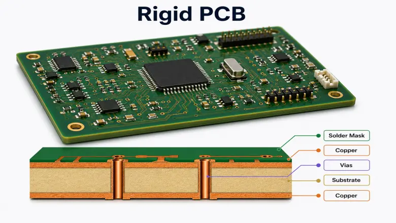
Rigid PCB
A rigid PCB uses a solid and inflexible substrate that holds its shape permanently once manufactured. It can be single-sided, double-sided, or multilayered depending on the application, but it always stays flat and can’t be bent or reshaped afterward.
Rigid boards are the most widely used type overall because most PCBs are required to be stable and durable. So, you can see these boards in computers, televisions, industrial control systems, automotive electronics, and medical equipment.
-
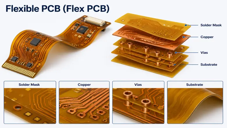
Flexible PCB (Flex PCB)
Flex PCBs swap the rigid substrate for a bendable material like polyimide, which lets the board fold or flex to fit unusual shapes inside a device. This flexibility makes them ideal for compact and space-constrained products like wearables and foldable electronics. However, they tend to cost more and are trickier to repair than rigid boards. They also come in single-sided, double-sided, and multi-layer variants.
-
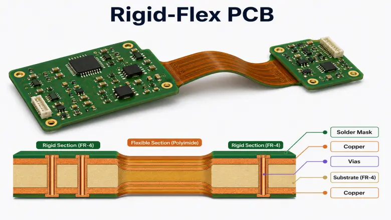
Rigid-Flex PCB
This printed circuit board (PCB) type combines rigid and flexible sections into a single integrated board. The rigid areas hold components in place, while the flexible sections allow parts of the board to bend or fold as needed. This approach cuts down on the connectors and wiring that would otherwise be needed to link separate boards. It’s a common choice in aerospace, medical devices, and other applications where durability and compact 3D design matter.
| Type | Layers | Flexibility | Cost | Best For |
| Single-Sided | 1 | Rigid | Low | Simple, low-density circuits |
| Double-Sided | 2 | Rigid | Low–Moderate | Consumer electronics |
| Multilayer | 3+ | Rigid | High | Smartphones, computers |
| Rigid PCB | 1, 2, or 3+ | None | Low | Mass production |
| Flex PCB | 1, 2, or 3+ | Bendable | High | Wearables, compact devices |
| Rigid-Flex | Mixed | Partial | Very High | Aerospace, medical devices |
PCB Manufacturing Process & Design Considerations
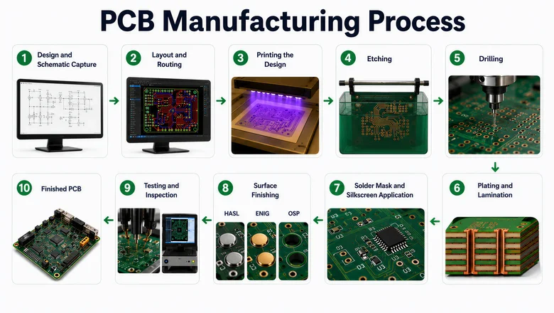
There is a consistent sequence of steps involved in the PCB (printed circuit board) manufacturing. The specifics can vary based on the design complexity, but the general process is as follows:
The Manufacturing Process
- Design and Schematic Capture: It starts with engineers laying out the circuit in design software. They define how every component connects and what the board needs to accomplish.
- Layout and Routing: The schematic is translated into an actual physical layout. This involves placing components and routing copper traces. Signal integrity and thermal behavior are kept in mind.
- Printing the Design: The finalized layout is transferred onto the copper-clad substrate using a photosensitive film and UV light to imprint the trace pattern.
- Etching: Chemicals strip away the unwanted copper and leave only the traces/pads and planes required in the design.
- Drilling: Holes are drilled for vias and component leads, which allow connections to pass between layers or accept through-hole parts.
- Plating and Lamination: Drilled holes get plated with copper to enable electrical continuity. For multilayer boards, individual layers are bonded together under heat and pressure.
- Solder Mask and Silkscreen Application: A protective solder mask is applied over the copper, followed by silkscreen printing for labels and component markers.
- Surface Finishing: A finish (HASL, ENIG, or OSP) is applied to exposed copper pads to protect them and improve solderability.
- Testing and Inspection: Finished boards go through electrical testing and visual or automated inspection to catch shorts or manufacturing defects before shipment.
Key Design Considerations
- Design for Manufacturability (DFM): Align the design with what a fabricator can actually produce early on to avoid rework and delays later.
- Signal Integrity: Ensure proper trace routing/width/spacing and layer stack-up to keep signals clean at higher speeds and frequencies.
- Thermal Management: Plan copper pours and thermal vias, along with component placement, to manage heat flow across the board.
- Power Distribution: Use dedicated power and ground planes to keep voltage delivery stable, especially in multilayer designs.
- Component Placement: Position parts thoughtfully to simplify routing and support thermal performance. It also eases assembly or rework.
- Industry Standards: Follow established guidelines to ensure the design meets accepted reliability and manufacturing benchmarks.
- Cost and Complexity Trade-offs: Balance layer count and tolerances against budget, since added performance usually comes with added cost.
How to Choose the Right PCB for Your Project
| Factor | What to Consider |
| Circuit Complexity |
|
| Space & Form Factor |
|
| Operating Environment |
|
| Signal & Power Needs |
|
| Reliability Standards |
|
| Budget & Production Volume |
|
| Manufacturer Capabilities |
|
What Do PCB Circuit Board Manufacturers Do
PCB circuit board manufacturers handle everything needed to turn a design file into a working board. What most manufacturers cover:
- Design Support and DFM Review: Many manufacturers review a design before production to flag manufacturability issues. They offer feedback or a formal DFM (Design for Manufacturability) report to prevent expensive errors down the line.
- Material Selection: Manufacturers help choose the right substrate (standard FR-4, high-frequency laminates, aluminum, or ceramic) based on thermal/electrical and cost requirements.
- Fabrication: Manufacturers handle etching, drilling, plating, laminating, and finishing the bare board according to the design’s specifications.
- Prototyping: Most manufacturers offer small-batch prototype runs first. They let engineers validate a design before beginning full production volumes.
- Component Sourcing: Many offer partial or full turnkey service. They can source some or all of the components listed in a bill of materials (BOM) on the customer’s behalf.
- Assembly: Manufacturers often handle populating it with components through SMT (surface-mount) or through-hole assembly methods.
- Testing and Inspection: Finished boards go through electrical testing or X-ray inspection to catch defects before shipping.
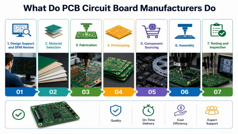
Manufacturers like LHD Tech reflect this full-service model well. We offer fabrication and assembly under one roof with no minimum order quantity, along with ISO, UL, and RoHS certification for projects that demand strict quality standards.
Overall, PCB circuit board manufacturers are usually full-service partners that join your team during initial design analysis and remain involved until the final board meets your technical and performance requirements.
Conclusion
The PCB printed circuit board can be the least visible part of any electronic device, but it offers the structure that combines separate components into a single working system. Every part of a PCB’s design plays a role in how reliably the device performs, which is why choosing the right board type and PCB circuit board manufacturer is essential for any electronics project.
FAQs
What is a printed PCB?
A printed PCB, or printed circuit board, is a flat board with copper traces etched onto an insulating base. It connects electronic components and holds them in place mechanically. It is the backbone of almost every electronic device.
What is the difference between PCB and PCBA?
A PCB (Printed Circuit Board) is the bare board that includes copper traces on a substrate, with no components attached. A PCBA (Printed Circuit Board Assembly) is that same board after components like resistors, transistors, ICs, and capacitors have been soldered onto it to make it fully functional.
How does a PCB work?
A PCB routes electrical current and signals through copper traces to connect components. As current flows along these predefined paths, each component performs its function and allows the whole board to work together as one circuit.
What is the 3W rule for PCB?
The 3W rule is a spacing guideline stating that the distance between the centers of two adjacent traces should be at least three times the trace width. This helps reduce crosstalk and signal interference between neighboring traces.