

A battery pack that delivers 100 A or more puts every millimeter of its management board under load. Each trace and via adds resistance, and that resistance turns into heat at a rate of current squared times ohms. Heavy copper PCB design keeps those losses low on a compact board, but thicker foil brings its own layout rules and fabrication limits.
This guide covers how to size copper for a high-current PCB design in a BMS and what a fabricator can realistically build, then looks at the layout details that decide whether a BMS board runs cool or fails in service.
What Is a Heavy Copper PCB?
A heavy copper PCB uses thicker copper conductors than conventional circuit boards. Standard boards commonly use 1 oz copper, but heavy copper designs usually start at 3 oz per square foot.
Copper weight describes the amount of copper distributed over a given area. For engineers, it provides an approximate indication of conductor thickness.
| Copper Weight | Nominal Thickness |
| 1 oz | 35 µm |
| 2 oz | 70 µm |
| 3 oz | 105 µm |
| 4 oz | 140 µm |
| 6 oz | 210 µm |
These are nominal values. Finished PCB thickness can vary with fabrication processes, particularly on plated outer layers.
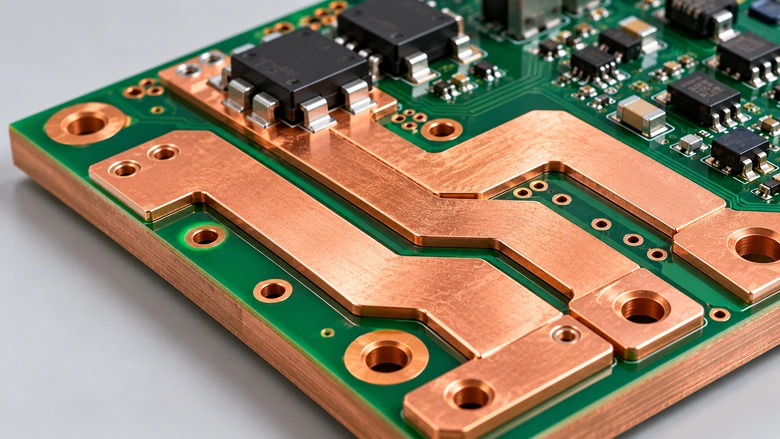
Increasing PCB copper thickness reduces resistance for a given trace width and length. This makes heavy copper PCB design useful in battery protection circuits, power switching sections, and other areas carrying substantial current.
Why High-Current BMS PCBs Need Thicker Copper
A BMS protects the cell from overcharge and over-discharge, and it opens the circuit during short circuits or overheating. Because the BMS sits in series with the pack, its components have to accommodate the full battery current. That makes the main discharge path the most demanding part of the board.
Heavy copper generally means 3 oz (about 105 µm) or more per layer, and extreme designs reach 20 oz and beyond. The advantage comes from cross-section, since thicker copper reduces electrical resistance, which allows high-current paths to carry power with less heat generation. Going from 1 oz to 2 oz usually halves the resistance along the same length of trace.
Let’s understand this with a quick example. Suppose a BMS board has a copper trace with these specifications:
- Copper thickness: 3 oz (105 µm)
- Trace width: 10 mm
- Trace length: 40 mm
- Current: 60 A
At 20°C, this trace has about 0.64 milliohms (mΩ) of resistance. Although that sounds small, carrying 60 A through it generates about 2.3 watts of heat.
If the same trace used 1 oz copper, its resistance and heat generation would be about three times higher under the same conditions.
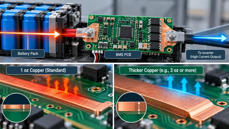
This explains why copper thickness matters in high-current BMS PCB applications. Wider, thicker traces help reduce electrical losses and temperature rise, although the final design still needs thermal testing.
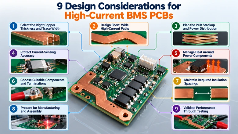
9 Design Considerations for High-Current BMS PCBs
The process of designing a heavy copper printed circuit board (PCB) for a high-current BMS involves more than choosing thicker copper. Engineers also need to consider how current moves through the board and where heat builds up.
The following considerations cover these decisions from initial layout through production testing.
1. Select the Right Copper Thickness and Trace Width
Copper weight depends on how much current the board must carry. Start with the continuous operating current and expected surge current. Then determine the allowable temperature rise and the space available for the power traces.
IPC-2152 provides guidance for estimating conductor dimensions based on current and temperature rise. The calculation must also account for the board’s construction and thermal conditions. For example, an internal trace dissipates heat in a different way from an exposed outer-layer trace, while nearby copper planes can influence its temperature.
The temperature around the conductor matters as well. Copper near the MOSFETs may already be warm before it carries its full operating current. Engineers should account for this local temperature when deciding how much additional heating is acceptable.
Heavy copper fabrication introduces another consideration about finished trace geometry. Etching can produce slightly tapered sidewalls, so the conductor’s actual cross-sectional area may differ from its nominal dimensions. Use the finished copper thickness and geometry when evaluating resistance and current capacity.
Verify the design under representative operating conditions, especially where cooling is limited.
2. Design Short, Wide High-Current Paths
Poor routing can cause localized heating even with thick copper. Long and narrow traces increase resistance. Sharp reductions in conductor width can also create bottlenecks, especially near MOSFET terminals and current-sensing components.
Good layout practices for heavy copper PCB design include:
- Keep high-current paths short and direct.
- Use wide copper areas where space allows and avoid narrow sections around MOSFET pads and current sensing resistors.
- Give parallel MOSFETs balanced power connections and suitable gate-drive routing to support current sharing.
- Size PCB-to-cable connections carefully, including connector terminals and solder joints.
For parallel MOSFETs, matching copper geometry helps reduce differences in electrical resistance. However, current sharing also depends on device characteristics, switching behavior, and temperature.
At very high currents, a separate busbar or another dedicated power conductor may be more practical than carrying the entire load through PCB traces.
3. Plan the PCB Stackup and Power Distribution
Multilayer construction allows designers to separate power paths from sensitive monitoring circuits. A multilayer PCB stackup might use heavier copper on selected power layers and maintain thinner copper for signal routing. This allows finer traces around monitoring ICs and reserves heavier copper for the main current paths.
Such mixed-copper constructions require fabrication review. The PCB manufacturer should verify that the proposed stackup can be fabricated reliably. Copper distribution must also be balanced to reduce warpage, while dielectric thickness and conductor spacing must meet the board’s insulation requirements.
Keep Sensitive Signals Away From Power Switching
High-current switching can interfere with voltage measurements and communication signals. Route sensitive traces away from MOSFET switching nodes and keep their connections direct.
A continuous ground reference plane can help reduce noise when it suits the circuit’s grounding design. Our PCB ground plane guide covers these considerations in more detail.
4. Protect Current-Sensing Accuracy
Many BMS designs measure battery current using a low-resistance shunt.
The measurement circuit detects a small voltage drop across the resistor and uses it to calculate current. Because the measured voltage is so small, resistance in solder joints and surrounding copper can introduce errors.
Use Kelvin Connections
Kelvin sensing separates the voltage measurement connections from the main current path.
The high-current terminals carry the battery current, while dedicated sense connections measure the voltage close to the resistor’s intended sensing points. This reduces the influence of voltage drops along nearby copper and solder connections.
Pad geometry is crucial here. Analog Devices has demonstrated that the placement of sense connections can affect measurement accuracy, which is common when conventional two-terminal shunt resistors are used.
Keep the sense traces away from noisy switching paths and route them as a closely coupled pair where appropriate. Vias may be used when the resistor footprint and circuit layout call for them. The exact connection points should follow the shunt resistor and measurement IC manufacturers’ recommendations.
Current-sensing accuracy should also be checked across the expected operating temperature range. Both the resistor’s characteristics and temperature differences across the assembly can influence the measurement.
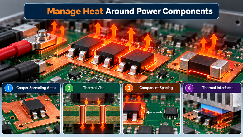
5. Manage Heat Around Power Components
Heavy copper PCB design for high-current BMS applications reduces conductor resistance, but it cannot eliminate heat generated by power devices.
MOSFETs, shunt resistors, and power connectors may still become hotspots. Their temperatures depend on electrical loading and the cooling conditions inside the battery enclosure.
Thermal management should begin with component placement and the available heat-transfer paths. Some of the useful design measures include:
- Copper spreading areas: Provide suitable copper around power components to distribute heat.
- Thermal vias: Connect copper layers to improve heat transfer where the component package and PCB construction allow.
- Component spacing: Keep temperature-sensitive monitoring components away from major hotspots.
- Thermal interfaces: Provide a defined heat-transfer path to a heatsink or enclosure when required.
Thermal via placement needs particular attention around MOSFETs. Vias placed in or near solderable thermal pads can affect soldering unless the footprint and via construction are designed for that arrangement.
Testing is essential because a board that runs comfortably on an open bench may become much hotter inside a sealed battery pack.
Thermal imaging and temperature measurements under representative loads can reveal hotspots around connectors/resistors and switching devices before production begins.
6. Design Vias and Connections for High Current
Vias are small plated holes that connect copper layers in a PCB. When high current passes through them, undersized vias can increase resistance and generate excess heat.
To prevent this, engineers should use enough vias to carry the required current and distribute them across the copper area. High-current designs may also need thicker via plating or larger plated holes, which depends on the electrical requirements and manufacturing capabilities.
Thermal relief connections also need attention. These narrow copper connections make soldering easier by reducing heat loss into large copper planes, but they can restrict current flow. For high-current pads, designers should check that the connections can handle the load or consider direct connections to the copper plane where soldering conditions allow.
7. Allow for Heavy Copper Manufacturing Constraints
Heavy copper changes how a PCB is fabricated. It takes more effort to etch, and material can be removed from the sides of the conductors as well as the exposed surface. This limits how close traces can be placed.
Minimum spacing requirements increase with copper thickness, although the exact dimensions vary between manufacturers. A layout that works with 1 oz copper may need wider gaps when produced with 4 oz or 6 oz copper.
Several other manufacturing details deserve attention:
- Copper build-up: The manufacturer may use heavy starting foil, along with additional plating or a combination of processes, to achieve the required finished thickness.
- Lamination: Resin must fill the spaces around thick internal copper features without leaving voids.
- Copper balance: Uneven copper distribution can contribute to distortion during fabrication.
- Plated holes: Hole dimensions and finished plating thickness must meet electrical and mechanical requirements.
- Solder mask: Tall copper features create additional challenges for coating coverage and registration.
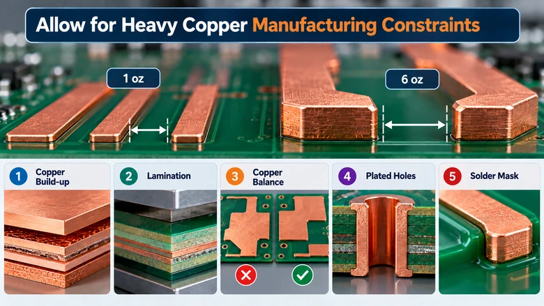
The manufacturing method affects achievable trace dimensions and tolerances, so confirm the fabricator’s design rules before routing the board. A design-for-manufacturing review should also examine the proposed stackup and spacing around high-voltage conductors.
8. Account for Soldering and Mechanical Reliability
Thick copper spreads heat well during operation, but it makes soldering harder. Large copper areas act as heat sinks that slow local heating, so pads on power connectors and other large components can take longer to reach solder temperature. The result is weak or inconsistent joints.
The manufacturer should adjust the reflow soldering profile to the board’s copper thickness and component layout. Thermocouples on the hottest and coldest solder joints show whether every joint reaches the right temperature. Solder paste volume also needs a check, and through-hole parts often need a method that delivers more heat to the barrel, such as selective soldering.
Mechanical strength matters just as much, especially where heavy cables connect to the board. Cable movement and vibration can crack solder joints over time. Secure connector mounting and proper strain relief keep that load off the joints.
9. Verify Current Capacity and Manufacturing Quality
A high-current BMS board should be tested under conditions close to its intended use. Electrical testing can identify opens/shorts and other manufacturing defects. However, verifying high-current performance requires additional measurements.
During qualification, engineers should check:
- Temperature rises at rated current.
- Voltage drops across critical power paths.
- Current-sensing accuracy.
- Connector and solder joint temperatures.
- Performance during representative current transients.
PCB inspection is also important. Automated optical inspection can identify visible assembly defects, while X-ray inspection helps examine hidden solder connections.
For critical designs, manufacturers may also use cross-section analysis to evaluate copper plating quality and internal construction.
Thermal cycling and other environmental tests can be included when required by the product’s operating conditions. The final qualification plan should reflect the battery system’s expected electrical loads and service environment.
Conclusion
Heavy copper PCB design for a high-current BMS depends on a chain of decisions that all have to hold up under load. Even with thicker copper, poorly sized traces or weak connections can lead to overheating and reliability problems. Careful layout and testing help catch these issues before production.
If you are developing a high-current BMS board, LHD TECH can help you turn your design into a manufacturable PCB. The company offers heavy copper PCB fabrication, multilayer manufacturing, and PCB assembly, along with engineering reviews to identify potential production challenges. Share your Gerber files, BOM, and copper thickness requirements with us to discuss your project and request a customized quote.