What Is PCB X-ray Inspection and Why Is It Crucial?
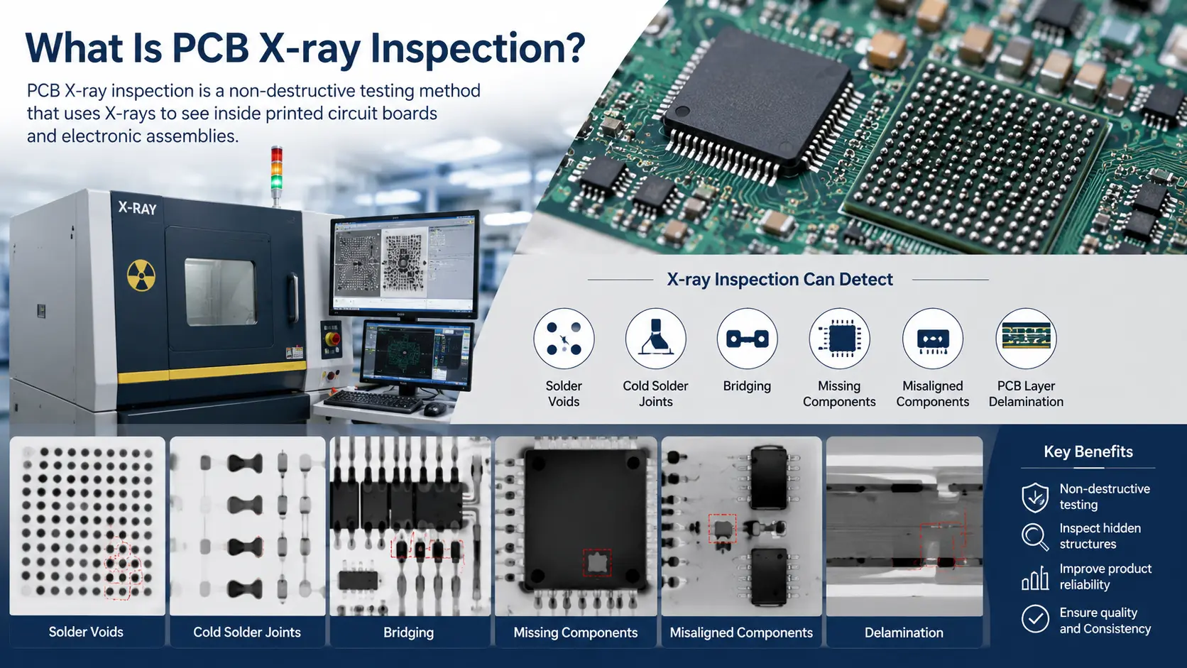
When you’re dealing with modern PCBs especially multi layer boards or designs with BGA packages a surface level look just doesn’t cut it. Traditional visual checks and even automated optical inspection (AOI) are limited to what’s visible on the outer layers; they rely on line of sight and can’t see through the board. That’s where X‑ray inspection comes into play. It’s a non‑destructive method that lets you peer right into the internal structure of the board, revealing details that no optical system could catch. By measuring variations in material density and thickness as X rays pass through different features, the system can flag hidden solder joint defects things like voids, misalignment, head‑in‑pillow, or shorts buried under components. The beauty of it is that you don’t have to destroy the board to get that information, which makes it invaluable for quality control, failure analysis, and process validation in high‑reliability applications.
Why Is X-ray Inspection Necessary for Modern PCBs?
Modern PCBs have become a whole different challenge. Components are getting tinier, board stacks now run multiple layers deep, and plenty of parts BGAs being a prime example have their terminations tucked underneath, completely invisible from the outside. That makes life tough for conventional inspection. Automated optical inspection (AOI) and manual visual checks are essentially surface‑bound; they rely on what’s optically reachable and can’t peer into the inner layers or under those packages. X‑ray technology changes the game entirely. It gives you sharp, high‑resolution magnified images that reveal exactly what’s going on inside voids, cracks, head in pillow joints, or any other anomaly that would otherwise stay hidden until the board fails in the field.
Key Benefits:
- Detects hidden and internal defects without damaging the PCB.
- Essential for inspecting complex PCBs and dense boards with BGAs, QFNs, and other bottom-terminated components.
- Supports quality control, process improvement, and compliance with industry standards like IPC-A-610.
How X-ray Inspection Works for PCBs
The Basics of X-ray PCB Inspection
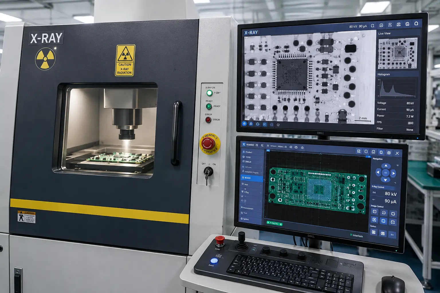
So why do we even bother with X ray inspection on PCBs? The short answer is: because we can’t see what’s really going on inside the board, especially with today’s multi‑layer designs and hidden interconnects. Here’s the basic physics behind it. The machine uses an X ray tube basically a controlled source that shoots a beam of high‑energy radiation down onto the assembled board. As that beam penetrates the PCB, it encounters all sorts of materials along the way, and each one reacts differently. The key factor is density: the more tightly packed the atoms, the harder it is for those rays to pass through. So when the beam hits a chunky solder joint or a solid copper trace, a lot of the radiation gets absorbed and doesn’t make it to the detector on the other side which is why those areas show up as bright white or light grey in the final image. On the flip side, the epoxy glass substrate is relatively low‑density, so most of the rays sail right through, appearing dark. And if there’s a void an air pocket trapped inside a solder joint that empty space offers almost no resistance at all, so it looks even darker, almost black. The detector captures all these variations in intensity and turns them into a grayscale image that tells you a whole lot more than just what’s on the surface. You get a clear picture of the top layer, sure but you also get a peek at the inner layers, the underside of BGAs, and the quality of plated through‑holes, all without having to cut, grind, or otherwise destroy the board. That’s the real beauty of it: you get full diagnostic visibility while keeping the board perfectly intact for further testing or actual use.
System Components:
- X-ray tube: Generates a beam of X-rays.
- Sample stage: Precisely positions the printed circuit board for inspection.
- Detector: Captures transmitted X-rays and converts them into detailed images.
- Software: Enhances, processes, and analyzes X-ray images—sometimes using AI to flag defects.
Magnification is achieved by adjusting the distance between the X-ray tube, sample, and detector, allowing operators to zoom in on tiny solder joints and components for detailed analysis.
Inside the Inspection Process
- Place the PCB on the sample holder or X-Y stage.
- Adjust settings: voltage (usually 80–160kV), current, exposure time, and magnification.
- Capture 2D images at multiple, often automated, positions and angles.
- (Optional) Perform advanced analysis, like laminography or 3D X-ray/CT, for volume reconstruction.
- Interpret images for inspection targets: voids, bridges, incomplete fills, and misalignment.
Safety Considerations
All industrial X-ray inspection systems incorporate shielding and interlocks, ensuring operators aren’t exposed to X-ray radiation. Always follow local safety regulations and training.
Types of X-ray Inspection: 2D, Laminography, and 3D X-ray
There are several approaches to X-ray PCB inspection, each appropriate for different challenges.
| X-ray Inspection | Description | Typical Use Case |
| 2D X-ray | Single-view, high-throughput top-down imaging | Inline inspection for solder voids, bridges |
| Laminography | Slices captured at different angles, reconstructing a 2.5D image | Detect internal layer misalignment, through-holes |
| 3D X-ray (CT) | Rotational scans and volume reconstruction | Failure analysis, hidden BGA/void root cause |
2D X-ray
Inline 2D X-ray inspection is fast and widely used in factories for scanning entire PCB assemblies for solder joint defects, voids, and gross misalignments.
Laminography
A technique between 2D and 3D, laminography records 2D images from different angles to focus on individual layers. It’s particularly useful for inspecting complex PCBs’ inner layers, barrel fill in through-hole components, and vias in dense boards.
3D X-ray / Computed Tomography
3D X-ray (CT) uses a rotational approach and multiple images from different angles to build a volumetric model. This enables engineers to examine the internal space of solder balls, track void percentage, and analyze inner layers non-destructively. Essential for failure analysis in high-reliability sectors.
Why X-ray Inspection Is Essential for Complex PCB Assemblies
Complex PCB assemblies—such as those found in aerospace, high-speed telecom, and automotive safety modules—feature BGAs,ball grid arrays, fine-pitch components, and multiple stacked circuit layers. In these products, hidden solder joints, deep vias, and internal layer registration are critical to both electrical and mechanical performance.
Problems Solved by X-ray Inspection Services
- Hidden Solder Voids: BGA, LGA, and QFN packages often develop voids beneath the surface that can’t be seen externally but can compromise circuit reliability or lead to intermittent failures.
- Alignment & Registration Issues: Internal misalignment (where vias don’t line up with buried pads) is impossible to spot without advanced X-ray inspection.
- Short Circuits: Solder bridging beneath package bodies is a primary failure mode in high-density boards and is only visible via X-ray.
A Step-by-Step PCB X-ray Inspection Workflow
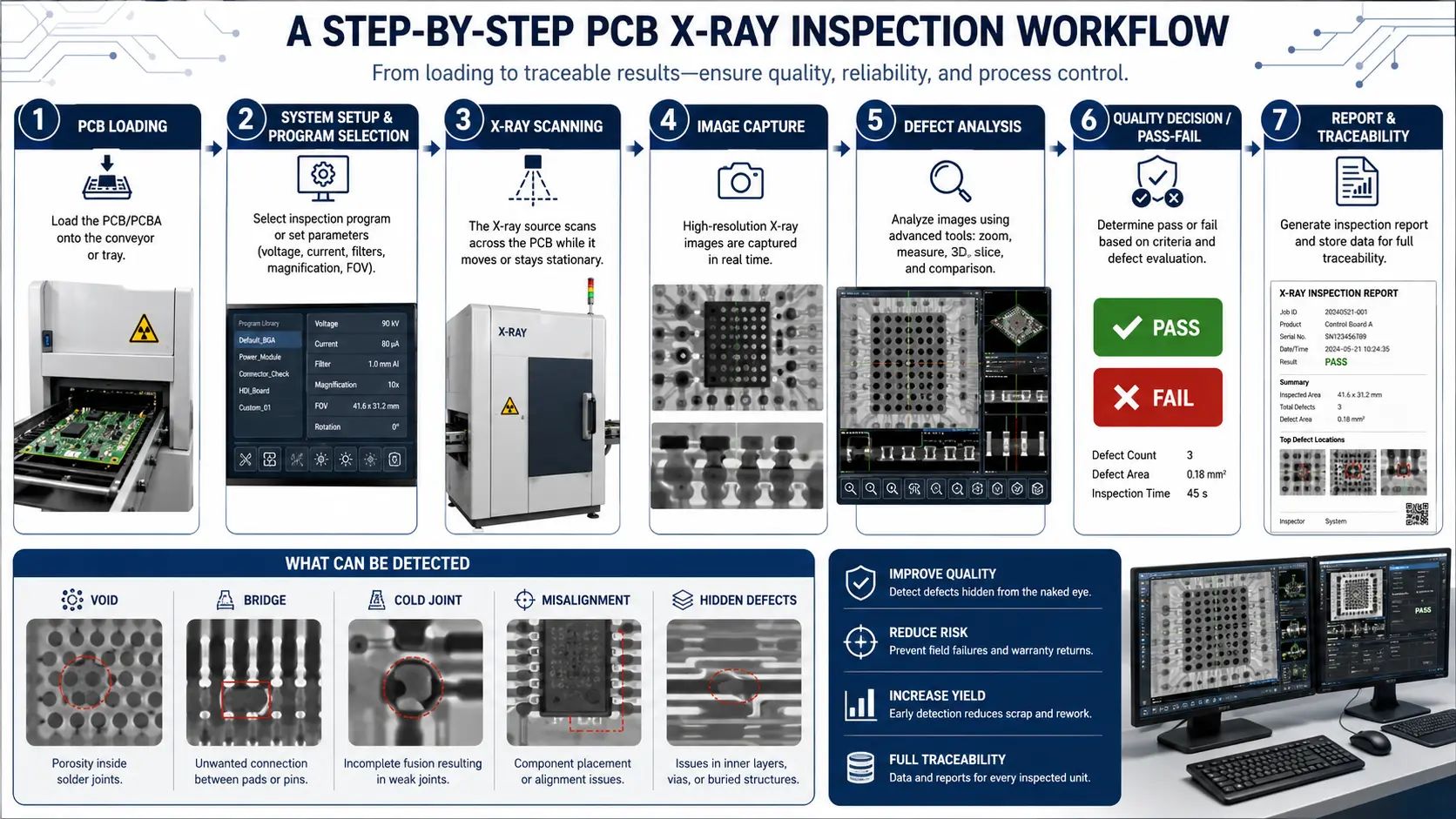
A disciplined inspection workflow ensures effective defect detection and traceability:
Start by going over the board layout and flagging the spots most likely to cause trouble.
Pay extra attention to BGA footprints, areas with dense component packing, via placements, and how well the barrel fill looks in through-hole vias these are where hidden defects tend to hide.
Define Inspection Scope and Criteria
Before you fire up the machine, you need to know what you’re looking for. That means pulling together IPCA610 standards and any customer‑specific requirements to set clear pass/fail thresholds for things like voiding, solder bridging, registration errors, and other common culprits.
Select the Proper Xray Inspection Technology
Your choice of equipment really depends on what you’re trying to achieve. For high‑throughput production lines, a 2D X‑ray system usually does the job. But if you’re doing root‑cause analysis or R&D work, you’ll want something more advanced – laminography or a 3D X‑ray system gives you the depth information you need.
Set Up the Xray Machine
With the system chosen, it’s time to dial everything in. Position the sample stage, tweak the X ray source parameters, and pick the right magnification and exposure settings. A few test shots at this stage can save you headaches later.
Capture Images at Different Angles
Don’t just settle for a straight top‑down view. Take oblique or tilted shots as well – they’re great for spotting solder bridges that might be hidden, checking how well the barrel fill looks, and getting a peek at what’s going on in the inner layers.
Analysis and Defect Classification
This is where the software earns its keep. Use it to measure void percentages, check solder ball alignment against the pads, and flag any defects – whether it’s a hidden solder joint issue, a bridge, a short, or misregistration. Experienced inspectors, backed by automated X‑ray inspection (AXI) algorithms, then compare the captured images against a known good “golden board” reference and the original design files to separate the real defects from false alarms.
Document Results and Maintain Traceability
For any board that goes through inspection – especially in aerospace, medical, or automotive sectors – you need a permanent record. Archive the X‑ray images along with lot numbers, test settings, and the findings. It’s not just good practice; it’s essential for audits, warranty investigations, and feeding back into process improvement loops.
Feedback to Assembly Process
The whole point of inspecting is to catch problems early. So when you spot excessive voids, barrel fill failures, or misaligned solder balls, don’t just log them and move on – push that information straight back to the assembly line. That way, you can adjust solder paste printing, tweak the reflow profile, or fine‑tune component placement before the next batch runs, which ultimately boosts your overall printed circuit board reliability.
Defects Detected Using PCB X-ray Inspection
PCB x-ray inspection makes it possible to uncover defects that escape other inspection methods including AOI and visual inspection. Here are key types of defects identified during x-ray PCB inspection and why they’re critical for quality control:
Common Defects:
- Solder Voids: Air pockets within solder joints—common under BGAs—that can weaken connections, cause resistance increases, or create long-term reliability issues.
- IPC-A-610limits void percentage, typically to ≤25% in critical joints.
- Solder Bridges: Unwanted solder connecting adjacent pads, often completely concealed in dense PCBs or beneath ball grid arrays.
- Open Joints and Head-in-Pillow Defects: Partial or incomplete fusion between a solder ball and its pad, especially in fine-pitch or lead-free assemblies.
- Barrel Fill Problems: Inadequate or uneven solder fill in through-hole connections, detected by angled x-ray images or laminography.
- Misalignment: BGA, LGA, or QFN package shifting, or inner layer via-to-pad registration failure.
- Component Lifting or Skew: Slight lifting caused by warpage, poor paste volume, or process anomalies.
- Blowholes or Cracks: Small, sub-surface voids in solder or minute cracks forming during reflow or handling.
| Defect Type | Impact on Circuit Boards | Detection With 2D/3D X-ray |
| Solder voids | Reliability loss, resistance increase | Excellent |
| Short circuits | Immediate or latent circuit failure | Excellent |
| Open joints | Intermittent faults | Good |
| Barrel fill issues | Incomplete electrical/mechanical connection | Excellent (2.5D/lamino) |
| Misalignment | Intermittent connection, early field failure | Excellent (3D/CT) |
| Cracks | Latent failure under thermal cycling | Good (high-res) |
Comparing Inspection Methods: AOI, Visual, and X-ray
Automated Optical Inspection (AOI)
- Pros: Fast, effective for surface inspection of solder joints and component placement.
- Cons: Cannot inspect hidden solder joints beneath BGAs or deep within multilayer PCBs.
Visual Inspection
- Pros: Simple, low-cost for accessible assemblies.
- Cons: Inefficient, inconsistent, and ineffective for high-density boards or internal features.
X-ray Inspection
- Pros: Reveals hidden defects like solder voids, short circuits, internal misalignment, and barrel fill issues. Delivers detailed images with high magnification for defect analysis.
- Cons: Higher upfront cost; requires advanced x-ray systems and trained operators.
| Feature | AOI | Visual Inspection | X-ray Inspection |
| Surface Defects | Yes | Yes | Yes |
| Hidden Defects | No | No | Yes |
| Throughput | High | Low | Medium–High |
| Defect Types | Cosmetic | Cosmetic | Cosmetic & Functional |
| Inspection As Part of Quality Control | Yes | Yes | Yes |
Cost and Business Impact of X-ray Inspection
Capital, Labor, and ROI
- CapEx: Modern inline 2D x-ray or 3D x-ray systems can cost from $80,000 to $400,000+. Advanced systems for failure analysis or high-mix, high-volume PCB manufacturing run higher but offer rapid defect detection, minimize rework, and increase first-pass yield.
- Opex: Operator training, image archival, and maintenance must be factored in.
- ROI Consideration: Reduces the risk of product recalls, costly field failures, high warranty costs, and brand reputation loss due to hidden solder joint and component defects.
Choosing a PCB Assembly Partner with X-ray Inspection Services
Carefully selecting a partner with industry-leading PCB x-ray inspection capabilities ensures higher product reliability, compliance, and customer satisfaction.
What to Ask Your Partner:
What types of X ray inspection systems are available in your facility? Do you operate inline automated machines for high‑volume production lines, or do you rely more on desktop units for offline sampling? And for deeper analysis – such as failure analysis or process development – do you have access to advanced CT (computed tomography) or laminography systems that can provide cross‑sectional or 3D volumetric data?
Do you support both 2D and 3D X‑ray imaging for fault isolation and root‑cause investigation? When we encounter an intermittent failure or a field return, we often need more than just a flat top‑down view. Can you provide 3D/CT scanning to pinpoint the exact location of a void, crack, or misalignment, and does your team have the expertise to interpret those 3D datasets effectively for root‑cause determination?
Is your entire X ray imaging process from image capture to archiving fully traceable and compliant with industry standards? We need to ensure that every inspection result is permanently stored with full metadata, including lot numbers, test parameters, and operator IDs. Beyond that, does your documentation meet the requirements of IPCA610 Class 2/3, and can you adapt to custom acceptance criteria specified by our customers?
Could you walk us through a real‑world example where your X ray workflow detected a hidden defect say, a void under a BGA or a barrel crack in a plated through hole and then explain how that information was fed back into your assembly process? We’re particularly interested in how quickly that feedback loop operates: does it trigger an immediate adjustment to solder paste printing, reflow profiling, or placement parameters, and how do you track the effectiveness of those corrective actions in reducing defect rates over time?
Tips, Case Studies, and Best Practices for Accurate X-ray PCB Inspection
- Predefine acceptance criteria: Set maximum allowable void percentage and define process triggers for real-time intervention.
- Train operators and engineers: Recognize natural variation (e.g. small, edge-located voids or intentional venting) versus real defects.
- Leverage magnification: Vary the stage and detector distances for optimal resolution—high magnification for BGAs, broader view for overall barrel fill.
- Keep systems calibrated: X-ray source and detector calibration guarantees the integrity and repeatability of every inspection.
- Data-driven improvement: Track recurring defects by component, batch, or placement machine to drive upstream fixes.
Future Trends in X-ray Technology and Inspection
The landscape of X-ray PCB inspection is rapidly evolving:
- AI-enhanced x-ray image analysis: Deep learning models now assist inspectors in highlighting and classifying subtle defects, reducing false negatives (missed hidden defects) and false positives.
- Inline 3D x-ray machines: Increasingly practical for more than just failure analysis—now entering high-volume production for complex PCB assemblies.
- Cloud-based archival and SPC integration: Immediate sharing of inspection results supports global, distributed PCB manufacturing.
- Higher-resolution detectors and micro-focus x-ray tubes: Offer sharper, more detailed images for even the most demanding fine-pitch BGAs.
Conclusion: Integrating PCB X-ray Inspection for Maximum Reliability
When you’re working with today’s high‑density printed circuit board assemblies, no other inspection method really comes close to what X ray technology can deliver in terms of visibility and diagnostic reliability. It gives you a window into the layers and joints that optical systems simply can’t see uncovering hidden problems like solder voids, bridges between pins, open connections that look fine on the surface, and components that have drifted out of alignment. Catching those issues before they leave the factory is what keeps product reliability high and failure rates low. And the benefits hold true across the board, whether you’re manufacturing avionics for aerospace, rugged PCBs for automotive applications, or compact, feature‑packed boards for consumer electronics. Making modern X ray inspection a standard part of your production line isn’t just about ticking a quality box – it directly leads to fewer field failures, lower recall costs, and stronger confidence from your customers. In short, it’s an investment that pays for itself many times over.
Take Action:
- Make x-ray inspection a core part of your quality control and assembly process.
- Insist on documented inspection methods and archived x-ray images per industry standards.
- Choose PCB manufacturing partners equipped with advanced x-ray machines, AI-driven analysis systems, and a robust workflow for preventing hidden defects.
FAQ: PCB X-Ray Inspection
1. What is X-ray inspection for PCBs?
PCB X-ray inspection is a non-destructive testing method that uses X-rays to examine internal solder joints, vias, components, and other structures that cannot be clearly inspected visually.
2. How does PCB X-ray inspection work?
X-rays pass through the PCB and are absorbed differently by materials such as copper, solder, and components. The resulting image reveals variations that can indicate internal defects or assembly problems.
3. What is a PCB X-ray inspection machine?
A PCB X-ray inspection machine is specialized equipment used to examine hidden structures and solder joints inside PCB assemblies. It is commonly used for BGA, QFN, CSP, and other components with concealed connections.
4. What defects can PCB X-ray inspection detect?
X-ray inspection can identify solder voids, bridges, insufficient solder, open joints, misalignment, missing balls, via defects, and other hidden PCB assembly issues.
5. How is PCB X-ray inspection performed?
The PCB or PCBA is placed inside an X-ray inspection system, where X-ray images are captured from selected areas. Inspectors or automated software then analyze the images for abnormalities and defects.
6. What components are commonly inspected using X-rays?
X-ray inspection is especially useful for BGAs, QFNs, CSPs, flip chips, and other components whose solder joints are located underneath the package and cannot be inspected directly by AOI.
7. What is PCB inspection?
PCB inspection is the process of checking bare boards or assembled PCBs for manufacturing and assembly defects. Common methods include visual inspection, AOI, X-ray inspection, electrical testing, and functional testing.
8. What are common PCB problems detected during inspection?
Common defects include solder bridges, insufficient solder, open joints, component misalignment, missing components, damaged vias, shorts, and solder voids. X-ray inspection is particularly effective for hidden defects.
9. How are PCBs tested for defects?
PCBs can be evaluated using AOI, X-ray inspection, flying probe testing, in-circuit testing, electrical testing, and functional testing. The appropriate method depends on the PCB design and defect type.
10. How much does a PCB X-ray inspection machine cost?
The cost varies significantly depending on resolution, inspection area, 2D or 3D capability, automation level, and software features. Advanced automated X-ray inspection systems generally cost more than basic manual systems.