A 6-layer PCB has two extra layers compared to a 4-layer PCB and delivers better signal control and reduced electromagnetic noise. This added layer count makes it easier to handle complex circuits, with extra routing and grounding flexibility. This guide will cover the 6-layer PCB stackup structure, manufacturing process, benefits, applications, and key factors to consider when choosing a 6-layer PCB manufacturer.
What Is a 6-Layer PCB?
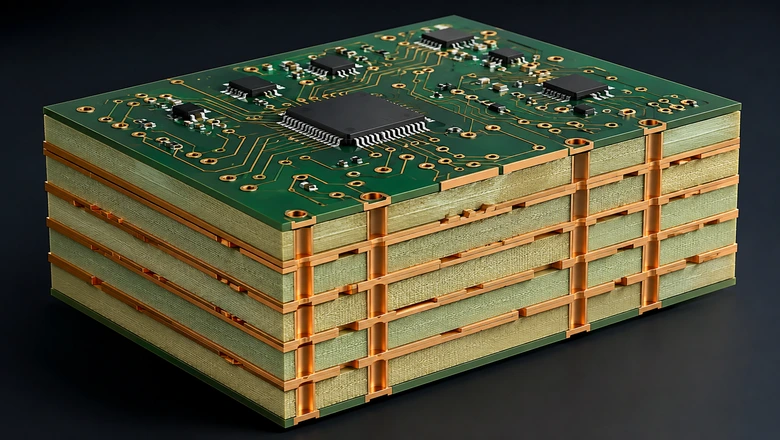
A 6-layer printed circuit board contains six separate copper foil layers, each bonded to the next with dielectric material in between. This structure provides six separate routing layers, which means multiple connection routes and more design options. This also leads to faster data transmission and better protection against power failures.

A 6-layer PCB board offers more space separating different parts of a circuit. This keeps the board compact while handling high component density in complex connections and high-speed signals.
The additional layers help achieve high electrical performance due to improved signal integrity, power distribution, and EMI control. This makes 6-layer PCBs common in network equipment, computers, industrial electronics, medical devices, and other applications where reliable performance is important.
| Technical Specifications of 6 Layer PCB | |
| Parameter | Approximate Value |
| Cooper weight | 1 oz – 2 oz |
| Board thickness | 0.8 mm – 2.0 mm |
| Dielectric thickness | 0.1 mm – 0.3 mm |
| Min Trace/Space | 4/4 mil (2/2 mil advanced) |
| Controlled impedance | 50Ω / 100Ω |
| Layer registration | ±0.075 mm |
| Drill tolerance | ±0.05 mm |
6-Layer PCB Stackup Structure
The 6-layer PCB stackup structure has a direct impact on EMI performance and impedance control. The right arrangement depends on routing density, signal speed, power requirements, and EMI considerations.
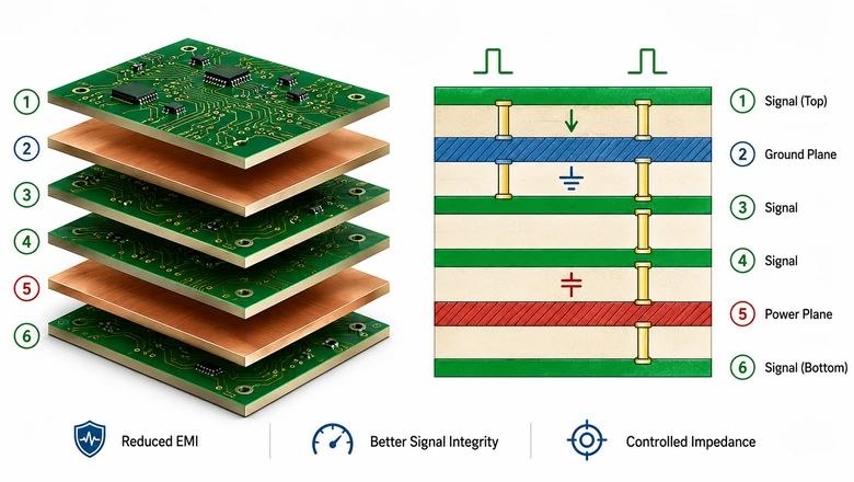
The standard stackup configuration is Signal–Ground–Signal–Signal–Power–Signal (S-G-S-S-P-S).
| Layer | Type | Function | Note |
| L1 | Signal layer | High-speed signal routing | Supports controlled-impedance traces |
| L2 | Ground plane | Signal return path | Helps reduce EMI and provides a low-inductance reference |
| L3 | Signal layer | Internal signal routing | Benefits from the adjacent ground reference layer |
| L4 | Signal layer | Internal signal routing | Suitable for differential pairs and other routed signals |
| L5 | Power plane | Power distribution | Provides a stable plane for supply voltages |
| L6 | Signal layer | Bottom-side routing | Used for component connections and shorter signal paths |
This multilayer arrangement provides high-speed signals with a stable ground reference to reduce electromagnetic interference and improve signal integrity.
6-Layer PCB Benefits
Despite just an addition of two layers to a standard 4-layer design, a 6-layer printed circuit board elevates every aspect of board performance.
More routing layers mean less congestion when packing in dense interconnections. Designers have more flexibility to keep analog/digital and power signals separated. That separation also improves signal paths because traces run with less distortion and better transmission efficiency.
The dedicated power and ground planes do work on the electrical side. A stable power distribution network drops voltage ripple. The 6-layer circuit board responds better to sudden changes in load due to a low-impedance path formed by paired power and ground planes. This is a genuine advantage for processors and other components switching at high speed.
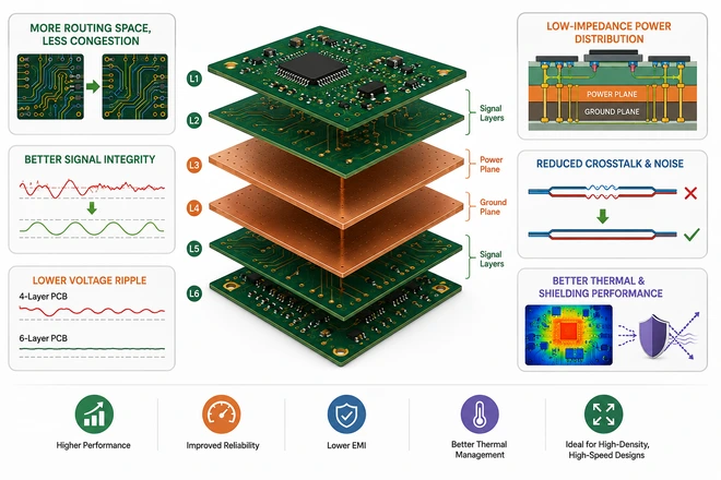
Ground planes also reduce crosstalk and noise between signal layers, which is essential in designs operating above 1 GHz because small interferences can cause real problems.
The extra copper in a 6-layer PCB stack offers thermal and shielding benefits. The packed copper planes help dissipate heat more effectively and keep the board reliable under sustained heavy loads.
6-Layer PCB Applications
The additional routing space and improved signal and power management make 6-layer PCB boards a good fit for electronic devices that are more complex than a typical 4-layer design can handle. They are found in high-speed and mixed-signal products to offer reliable performance and controlled signal routing.
- Telecommunications & Networking: Used in routers, switches, modems, and 5G equipment that handle high-speed data signals.
- Computing Equipment: Suitable for servers, embedded computers, motherboards, and other systems with high-speed interfaces and dense routing requirements.
- Automotive Electronics: Used in ADAS, ECUs, infotainment systems, and EV battery management systems where signal integrity and EMI control are important.
- Medical Devices: Found in monitoring and diagnostic/imaging equipment that requires accurate signals and reliable operation.
- Industrial Control: Used in PLCs, robotics, motor controllers, and factory automation equipment where power and signal circuits need to coexist on the same board.
- Consumer Electronics: Useful in smartphones, tablets, wearables, gaming devices, and other compact products that combine dense circuitry with high-speed interfaces.
4-Layer PCB vs 6 Layer PCB
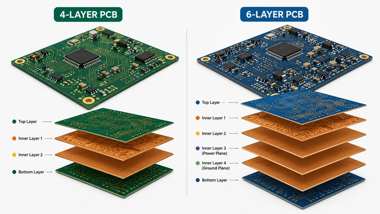
A 4-layer PCB is usually enough for moderately complex electronics. A 6-layer PCB board provides additional routing and power-management flexibility for denser designs. The right choice between the two relies on the circuit’s complexity, performance requirements, available space, and budget.
| Feature | 4-Layer PCB | 6-Layer PCB |
| Routing space | Moderate | Higher |
| Signal integrity | Good | Better |
| EMI control | Good | Better |
| Circuit complexity | Moderate | High |
| Board size | Compact | Compact |
| Manufacturing cost | Lower | Higher |
| Design flexibility | Good | Higher |
| Best for | General electronics | High-density, high-speed designs |
6-Layer PCB Thickness and Material Options
Board thickness and material choice have a direct influence on how a 6-layer circuit board performs mechanically/electrically. The right choice is linked to durability and minimized signal loss in high-frequency designs.
Standard board thickness usually sits around 1.6mm, though designs can go up to 2.0mm for added rigidity or down to 0.8–1.2mm for more compact builds. Material choice comes down to standard FR-4 or high-Tg laminates for boards facing more heat. It can also be RF-grade substrates like Rogers materials for RF and microwave applications.
Copper weight ranges from 1oz to 2oz depending on how much current or heat the board needs to handle. Thicker copper does mean etching has to be controlled more precisely to keep trace patterns accurate.
6-Layer PCB Manufacturing Process
Every additional layer on a PCB adds a new opportunity for something to go wrong. This is why 6-layer manufacturing follows a more disciplined process. The two extra inner layers have to be etched and inspected thoroughly before they are sealed inside the board.
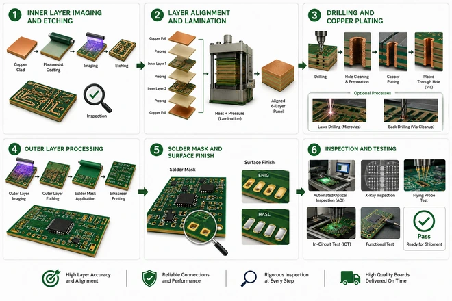
1. Inner Layer Imaging and Etching
The inner copper layers are coated with photoresist and exposed to the required circuit pattern. Unwanted copper is then etched away, which leaves the traces and planes of the desired design. Each inner layer is inspected before moving forward.
2. Layer Alignment and Lamination
The completed inner layers are stacked with prepreg and copper foil using precise registration tooling. Heat and pressure cure the prepreg resin and bond the layers into one rigid panel. Proper alignment is critical because errors at this stage can affect vias and connections throughout the board.
3. Drilling and Copper Plating
After lamination, holes are drilled for through-hole components and vias. The holes are cleaned and prepared before copper is deposited within them to create conductive paths between the required layers. Additional laser drilling or back drilling processes may also be used depending on the requirements.
4. Outer Layer Processing
The outer copper layers are patterned and etched to form the required traces and pads. Solder mask is then applied to protect exposed copper, while silkscreen adds component references and other markings.
5. Solder Mask and Surface Finish
A solder mask is applied to protect the copper from oxidation and short circuits. Also, a surface finish such as ENIG or HASL is applied to exposed pads to protect the copper and maintain solderability.
6. Inspection and Testing
The finished boards then undergo inspections and electrical testing to identify opens, shorts, alignment issues, or other manufacturing defects before shipment.
Read more: What Are The 7 Types Of PCB Testing Methods
Choosing the Right 6-Layer PCB Manufacturer
The complexity of a 6-layer PCB makes the choice of manufacturer more crucial and beyond just finding the lowest quote. A capable supplier should be able to work with your required materials, layer structure, trace widths, vias, impedance targets, and board thickness.
Consider these factors when choosing a 6-layer PCB manufacturer:
- Manufacturing capability: Check the manufacturer’s layer-count range, minimum trace and spacing, via options, copper thickness, and material choices.
- Quality control: Look for processes such as AOI, electrical testing, X-ray inspection, and documented quality standards.
- DFM support: A manufacturer that reviews your design before production can identify stackup, spacing, drilling, and manufacturability issues early.
- Lead time: Compare realistic prototype and production timelines.
- Production volume: Make sure the supplier can handle your expected order size (small batches to full production).
- PCB assembly: If you also need component placement and testing, use a manufacturer that offers fabrication and assembly to simplify the process.
LHD Tech is one reliable 6-layer PCB manufacturer that offers custom multilayer PCB fabrication, rapid prototyping, impedance-controlled designs, and turnkey PCB assembly. The company supports complex stackups, high-density interconnects, blind and buried vias, microvias, and a range of materials.
LHD Tech also provides DFM and engineering reviews to help identify layout, drilling, stackup, and manufacturability issues before production. There is no minimum order quantity requirement. The company also provides component sourcing, SMT and through-hole assembly, testing, and final product delivery as part of its one-stop PCB manufacturing service.
Bottom Line
A 6-layer PCB offers the extra routing space with signal control and power distribution needed for more demanding electronic designs. It provides a practical balance between performance and board size but requires the right stackup and a manufacturing partner, such as LHD Tech, to achieve reliable results.
FAQs
Is a 6 layer PCB bad?
Not, it’s actually a step up from a basic 4-layer board. You would only call it “bad” if your design doesn’t need the extra layers, since you would be paying for routing space and EMI control your circuit never actually uses.
How much does a 6 layer PCB cost?
There is no fixed number. The cost depends on board size, material, copper weight, and order quantity. Expect to pay more than for a 4-layer board due to the added lamination and drilling steps, but less than for 8 or more layers.