Every piece of domestic and industrial equipment that relies on electronics involves printed circuit boards (PCBs). However, before a circuit board ends up in any device, it must undergo a proper manufacturing process at a PCB factory. The level of precision that goes into that process is exceptional.
This guide breaks down what a PCB board factory actually does and uncovers everything that happens on the production floor. You will also learn how to separate a reliable factory from others.
What Is a PCB Factory?
A PCB factory is a facility that fabricates bare printed circuit boards. It turns raw copper, laminate, and resin into a finished board.
It transforms a digital design into a physical board ready to have components soldered onto it. However, the important distinction to clarify up front is between “PCB factory” and “PCB assembly company,” as these terms are often mixed up.
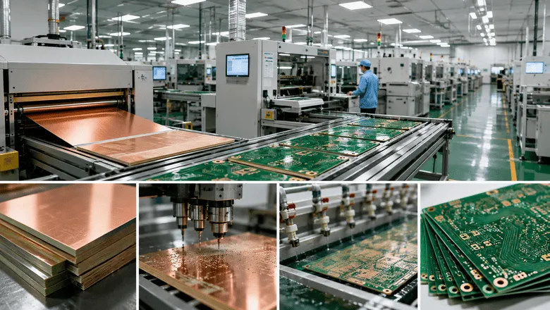
A PCB factory builds the board itself. A PCB assembly manufacturer populates that board with actual components. Many factories today handle both fabrication and assembly under one roof, which is usually called PCB turnkey manufacturing. However, the primary job of a PCB factory is to produce a bare board.
What Does a PCB Factory Actually Do?
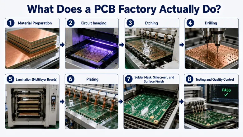
A Printed Circuit Board (PCB) factory follows a series of controlled steps to turn raw materials into a finished bare board. The exact process may vary depending on the board’s layer count and design, but the common approach involves:
-
Material Preparation
It all starts with the substrate (PCB laminate), usually FR-4 because it offers a good balance of cost and mechanical strength, along with reliable electrical insulation. However, high-frequency or high-temperature applications may require specialty laminates instead. The copper-clad panels are cut to the required size and prepared for the manufacturing process.
-
Circuit Imaging
Next, the circuit pattern is then etched onto the copper layer. This is performed using a photoresist and either traditional film exposure or Laser Direct Imaging (LDI). LDI provides greater registration accuracy and is required in dense and fine-pitch HDI boards.
-
Etching
After pattern exposure, the undesired copper is etched away chemically and leaves only the traces defined in the design. The etching process needs close control of factors such as chemical concentration, temperature, and conveyor speed. Even small variations can affect trace width and the board’s electrical performance.
-
Drilling
The panels are then drilled to create the holes needed for vias and component leads. This creates the pathways that will help connect different layers of the board electrically.
-
Lamination (Multilayer Boards)
Multilayer boards require an additional lamination step. The etched inner layers are aligned and stacked with sheets of prepreg before being pressed together under heat and pressure. The prepreg melts and bonds the layers into a single panel. This step only happens after those layers pass inspection.
-
Plating
Drilled holes are plated with copper to establish electrical continuity between layers. The outer layers are then formed through another imaging and etching process to create the final circuit pattern.
-
Solder Mask, Silkscreen, and Surface Finish
A solder mask is applied over the board to protect the copper and help prevent solder bridges and oxidation. Silkscreen is added for reference markings and component labels.
A surface finish, such as HASL or ENIG, is applied to exposed copper pads to protect them and maintain their suitability for soldering.
-
Testing and Quality Control
Before the boards leave the factory, they go through inspection and electrical testing. This can include automated optical inspection (AOI), flying-probe testing, or fixture-based electrical testing. The testing catches manufacturing defects and verifies that the finished board meets the required specifications.
Key Equipment Used Inside a PCB Factory
Behind each of the above manufacturing steps in a PCB factory, there is a lineup of specialized equipment. Some of the machines are highly automated, while others are for specific testing or production requirements. A few of the most important ones include:
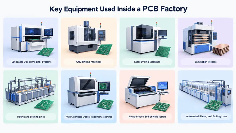
- LDI (Laser Direct Imaging) Systems: These systems use lasers to transfer circuit patterns onto the panel. They offer better registration accuracy than traditional film-based imaging and are useful for fine-pitch and HDI boards.
- CNC Drilling Machines: Drill the holes required for vias, component leads, and other mechanical features with precise positioning.
- Laser Drilling Machines: Create tiny microvias for HDI and other high-density boards where conventional mechanical drilling isn’t useful.
- Lamination Presses: Bond multiple PCB layers together using controlled heat and pressure to form a solid multilayer board.
- Plating and Etching Lines: Add copper to drilled holes and board surfaces, then remove unwanted copper to form the final circuit traces.
- AOI (Automated Optical Inspection) Machines: Use cameras to inspect circuit patterns and identify defects such as broken traces, shorts, and spacing issues.
- Flying-Probe / Bed-of-Nails Testers: Check electrical connections on finished boards. Flying probes suit prototypes and smaller runs, while bed-of-nails testers are used for higher-volume production.
- Automated Plating and Etching Lines: These systems move panels through a series of chemical processing stages with minimal manual handling. Automation helps maintain consistent process conditions across large production batches and reduces variation from one panel to the next.
Types of Boards a PCB Factory Can Produce
The types of PCBs each PCB board factory can produce can vary, but the capabilities fall into a few common categories:
- Single- and double-sided boards: Simple and lower-cost boards for basic circuits.
- Multilayer boards: Three or more layers, standard for smartphones and computers. Some can even produce 6-layer PCBs used in network equipment and industrial electronics.
- HDI (High-Density Interconnect) Boards: Boards made with microvias and fine traces for very compact, high-pin-count designs.
- Flex and Rigid-Flex Boards: Boards that bend or combine rigid and flexible sections for unusual form factors.
- High-Frequency Boards: Boards made on RF-grade laminates for telecom infrastructure and radar systems.
Quality Control in a PCB Factory
Quality control isn’t happening just at the start of selecting PCB material or at the end of production. It’s built into almost every stage of the process. For example, inner layers are inspected with AOI before lamination because a defect sealed inside a multilayer board has no way to fix it.
Finished boards also undergo electrical testing with flying-probe or bed-of-nails testers to check for open and short circuits. Factories may also inspect finished boards against industry standards such as IPC-A-600, which covers requirements for PCB workmanship and characteristics such as plating and annular rings.
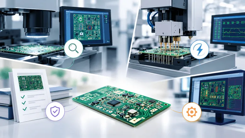
Many factories also offer DFM (Design for Manufacturability) reviews before production begins. These reviews can flag design features that may be difficult or costly to manufacture. Catching a problem in the design file is almost always easier than discovering it after the board has already
How to Choose the Right PCB Factory
There are many PCB factories businesses can choose from. However, compare the following aspects before committing to anyone:
- Certifications: ISO, UL, and RoHS compliance matter, especially for medical, automotive, or industrial applications with strict regulatory requirements.
- Technical Capabilities: Confirm the factory can actually produce your required layer count and trace width.
- DFM Support: A factory that reviews designs before production tends to catch costly mistakes early.
- Turnaround Time: Prototype runs and mass production have very different lead times, so clarify both upfront.
- Minimum Order Quantity: Some factories require large minimum orders, which can be a dealbreaker for prototyping or small-batch projects.
- Communication and Support: A factory that’s responsive and easy to work with makes the entire process smoother.
Conclusion
A PCB factory operates quietly in the background of the electronics industry. However, the precision happening on that production floor is what makes boards reliable.
If you are looking for a PCB board factory that takes service depth and quality seriously, LHD Tech combines fabrication and assembly with rigorous quality control and no MOQ restrictions. Reach out to see how we can support your next build.