A 2-layer PCB may no longer provide enough space for routing and power management when a PCB design becomes more complex. A 4-layer PCB adds two internal layers that can be used for power/ground and signal routing without having a noticeable increase in the board’s footprint.
A 4-layer PCB has become a common circuit board in consumer electronics and industrial equipment to improve performance and reliability. This guide will cover 4-layers PCB design, manufacturing, benefits, applications, and how to choose the right 4-layer PCB manufacturer.
What is a 4-Layer PCB?
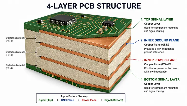
A 4-layer PCB (printed circuit board) consists of four separate copper foil layers, bonded together with insulating dielectric material sandwiched in between. The two outer layers are used for component mounting and signal traces, while the two inner layers are usually dedicated to power and ground planes. The thickness of a 4-layer circuit board is usually 0.13-0.15 mm, but you may also find thicker boards of 0.20-0.25 mm.
The internal planes in a 4-layers PCB give signals a stable and low-noise reference to travel against, which is useful during high-speed or mixed-signal circuits. Compared to a 2-layer board, it provides more room to route traces and cleaner return paths for fast signals. Compared to a 6-layer board, it offers cost-effective and faster fabrication, but it comes with fewer layers and routing headroom.
4-layer printed circuit boards are also suitable in a wide range of applications, including consumer electronics, industrial control systems, automotive electronics, telecommunications equipment, medical devices, and embedded systems.
The Functions of Each 4 Layer Circuit Board
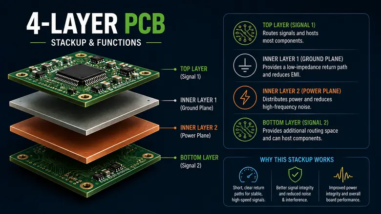
The most common 4 layers PCB design involves the top and bottom layers handling signal routing and component connections, while the two inner layers handle ground and power distribution.
Top Layer (Signal 1)
This outer layer carries high-speed signals and hosts most of the board’s components. It is the primary surface where routing and part placement happen.
Inner Layer 1 (Ground Plane)
This layer sits behind the top layer and provides a low-impedance return path for signals. It is essential for keeping fast digital signals clean and predictable. Placing it right next to a signal layer gives that layer a stable ground reference, which is valuable for high-speed and single-ended signals and helps control EMI.
Inner Layer 2 (Power Plane)
This layer distributes power across the board and supplies the voltage components need. Its close proximity to the ground plane creates interplane capacitance, which helps reduce high-frequency power noise and improves power integrity.
Bottom Layer (Signal 2)
The final layer offers additional routing space for signals. Like the top layer, it can also hold components depending on the design.
The Importance of This Specific 4-Layer Stackup Order
Signal layers next to ground or power planes give return currents a short and clear path. This helps keep signals stable and reduces unwanted noise.
Keeping the traces close to the ground plane can improve signal integrity for high-speed signals. Separating sensitive analog and digital circuit signals can also help reduce interference.
So, the extra layers in a 4-layer PCB do more than just provide additional routing space. The layer arrangement also helps board performance and grounding, plus signal quality.
4-Layer PCB Benefits
A 4-layer PCB provides better signal integrity and EMI control than a 2-layer design. The dedicated power and ground planes give signals a more stable reference, while also helping reduce noise and crosstalk.
The extra layers also make it easier to fit more components and traces into a smaller board. At the same time, a dedicated power plane helps distribute voltage more consistently across the circuit.
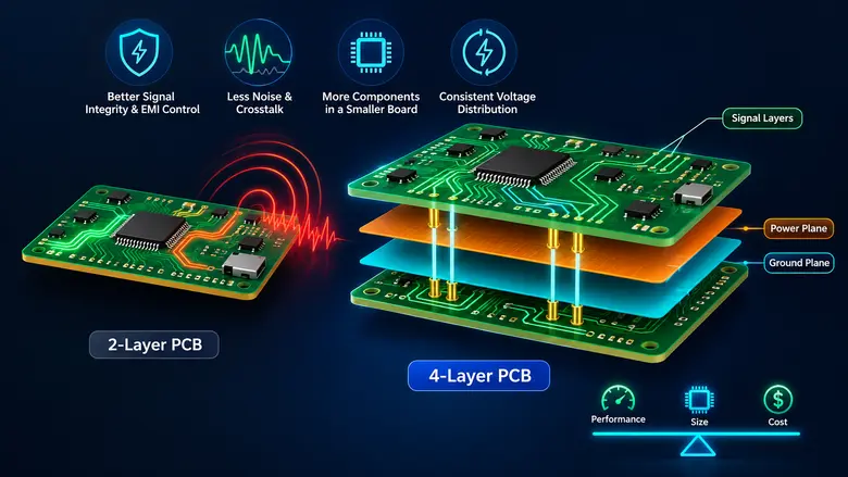
A 4-layer PCB can offer a good balance between performance/size/cost in complex designs. It provides more routing and grounding options than a 2-layer board without the added expense of moving to a higher-layer stackup.
4–Layer PCB Applications
The common 4-layers PCB applications include:
- Consumer electronics: Used in smartphones, tablets, laptops, smartwatches, gaming devices, and home appliances.
- Computers and peripherals: Found in motherboards, file servers, storage systems, printers, scanners, and other computer hardware.
- Telecommunications: Used in routers, switches, modems, repeaters, fiber-optic equipment, and wireless communication systems.
- Automotive electronics: Supports engine control units, infotainment systems, navigation systems, sensors, and driver-assistance technologies.
- Medical equipment: Used in heart monitors, patient-monitoring systems, hearing aids, diagnostic devices, X-ray equipment, and imaging systems.
- Industrial control systems: Applied in programmable logic controllers, automation modules, motor controls, power supplies, and security systems.
- IoT devices: Used in smart-home products, connected sensors, wearable devices, and remote-monitoring equipment.
- Power electronics: Suitable for UPS systems, power inverters, electricity-testing equipment, and other power-management applications.
- Aerospace and defense: Used in avionics, satellite equipment, navigation systems, military communication devices, and monitoring systems.
- High-speed digital and mixed-signal systems: Supports interfaces and circuits involving USB, HDMI, Ethernet, LVDS, RF, and other high-speed signals.
4-layer PCBs are used in all the above areas due to the additional routing space and dedicated power/ground planes. Plus, the improved signal integrity and reduced electromagnetic interference also come to their advantage.
2-Layer vs 4-Layer PCB
2-layer and 4-layer PCBs are the most common types of multiple-layer circuit boards. The choice between the two depends on the project’s complexity and space/signal requirements.
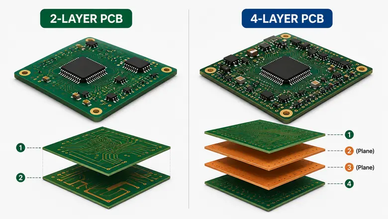
The difference between the two is summarized in the table below:
| Feature | 2-Layer PCB | 4-Layer PCB |
| Construction | Two copper layers | Four copper layers |
| Design complexity | Low | Moderate to high |
| Routing space | Limited | Expanded |
| Signal integrity | Suitable for basic circuits | Better for high-speed signals |
| EMI control | Basic | Improved |
| Power distribution | Less efficient | More stable |
| Board size | May require more space | Supports compact designs |
| Manufacturing cost | Lower | Higher |
| Use cases | Simple electronics and prototypes | Computers, IoT, automotive, and industrial systems |
| Best suited | Low-complexity projects | High-performance complex designs |
4-Layer PCB Manufacturing Process
The 4-layer PCB manufacturing process involves several steps because the inner copper layers are buried inside the board during lamination. The exact process can vary by manufacturer, but it follows these stages:
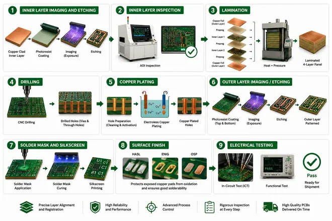
1. Inner Layer Imaging and Etching
The inner copper layers are coated with a photosensitive film and exposed to the circuit pattern. The unwanted copper is then etched away, which leaves the required traces and planes.
2. Inner Layer Inspection
The etched inner layers are inspected using automated optical inspection (AOI) to identify defects such as broken traces or incorrect patterns before the layers are laminated together.
3. Lamination
Stacking of inner layers is made with prepreg along with outer copper foils, then bonded together using heat and pressure. Precise alignment is important to ensure the layers and future drilled connections line up correctly.
4. Drilling
After the board is laminated, holes are drilled for vias and through-hole components. These holes provide the paths needed to connect the different copper layers.
5. Copper Plating
A thin layer of copper is deposited over the board surface and inside the drilled holes. This creates electrical connections between the different layers.
6. Outer Layer Imaging/Etching
The outer copper layers are patterned using imaging and etching. This creates the required signal traces/pads and other copper features on the top and bottom surfaces.
7. Solder Mask and Silkscreen
A solder mask is applied to protect the copper and prevent unwanted solder connections. Silkscreen is then added for component labels and other identification details.
8. Surface Finish
The exposed copper pads receive a surface finish to protect them from oxidation and maintain good solderability. Common options include HASL, ENIG, and OSP.
9. Electrical Testing
The finished PCB is electrically tested to check for open or short circuits and verify that the board meets the required design specifications before shipment.
Four-layer PCBs are more complex than standard two-layer boards. However, partnering with an experienced 4-layer PCB manufacturer can ensure you receive the high-quality boards required for your next project.
4-Layer PCB Manufacturers
There are many 4-layer PCB manufacturers available to fulfill your design requirements, but choosing the right one requires comparing beyond the lowest quote. Look at the manufacturer’s production capabilities, quality controls, turnaround times, and ability to support your project’s entire journey.
Cost: Compare quotes from several manufacturers, but check what is included in the price. Your final cost can be influenced by material selection, surface finish, testing, and shipping.
Quality and certifications: Check whether the manufacturer follows recognized standards such as ISO, UL, RoHS, and IPC. Also, ask about its inspection and testing methods.
Lead time: Ask for realistic prototype and production lead times. A manufacturer with good production capacity and clear communication can help prevent delays.
Order volume: Minimum order requirements can be a concern for prototypes and small production runs. Look for manufacturers that can handle your expected volume without forcing you to order more boards than you need.
Engineering and customer support: Good technical support can make the manufacturing process much smoother. DFM checks, stackup guidance, design review, and a dedicated point of contact can help identify problems before production begins.
LHD Tech is one reputed manufacturer that covers both PCB fabrication and assembly. The company supports PCB production from 1 to 42 layers and provides services from PCB manufacturing and assembly to testing and engineering support. It has ISO 9001, ISO 14001, UL, RoHS, and other quality certifications, along with no minimum order quantity for PCB manufacturing.
Bottom Line
A 4-layer PCB offers a balance of performance, size, and cost for modern electronic devices. The improved routing space and power distribution, along with signal integrity and EMI control, give it a wide range of applications. Therefore, it’s time to select a reliable 4-layer PCB manufacturer like LHD Tech and begin reliable production and consistent quality outcomes.
FAQs
How to layer a 4-layer PCB?
A usual 4-layer PCB uses the top layer for components and signal routing, the first inner layer for ground, the second inner layer for power distribution, and the bottom layer for additional signals and components. This arrangement supports cleaner signal return paths and improved power integrity.
When should I switch to a 4 layer PCB?
Switch to a 4-layer PCB when a 2-layer design lacks routing space or requires better power distribution. The switch also becomes essential when you experience signal integrity and electromagnetic interference issues. It is also suitable for high-speed or component-dense designs for reliable performance.
How thick are 4 layer PCBs?
The thickness of a 4-layer PCB depends on the manufacturer, materials, copper weight, and application requirements. Common options include approximately 0.13–0.15 mm for thinner boards and 0.20–0.25 mm for thicker designs.
What is the standard 4-layer PCB stackup?
The most common stackup is signal–ground–power–signal. The top and bottom layers carry components and signal traces, while the inner ground and power planes provide stable references.