Introduction: The Challenge of Finding the Right Manufacturer
In 2026, the demand for ultra-reliable, high-performance, high-density interconnect circuit boards has reached an all-time high. HDI PCBs are widely used across smartphones, wearables, AI servers, automotive electronics, and medical devices. Yet, the difference between a failed prototype and a market-defining product often boils down to one decision: selecting the right manufacturer.
Many would-be buyers make the costly mistake of focusing exclusively on the largest PCB manufacturer or pcb suppliers in China simply because they appear at the top of a search for “pcb manufacturer” or “top hdi pcb manufacturers.” In truth, project success depends on much more—certification, process control, engineering feedback, reliability testing, and manufacturing solutions tailored to your industry needs.
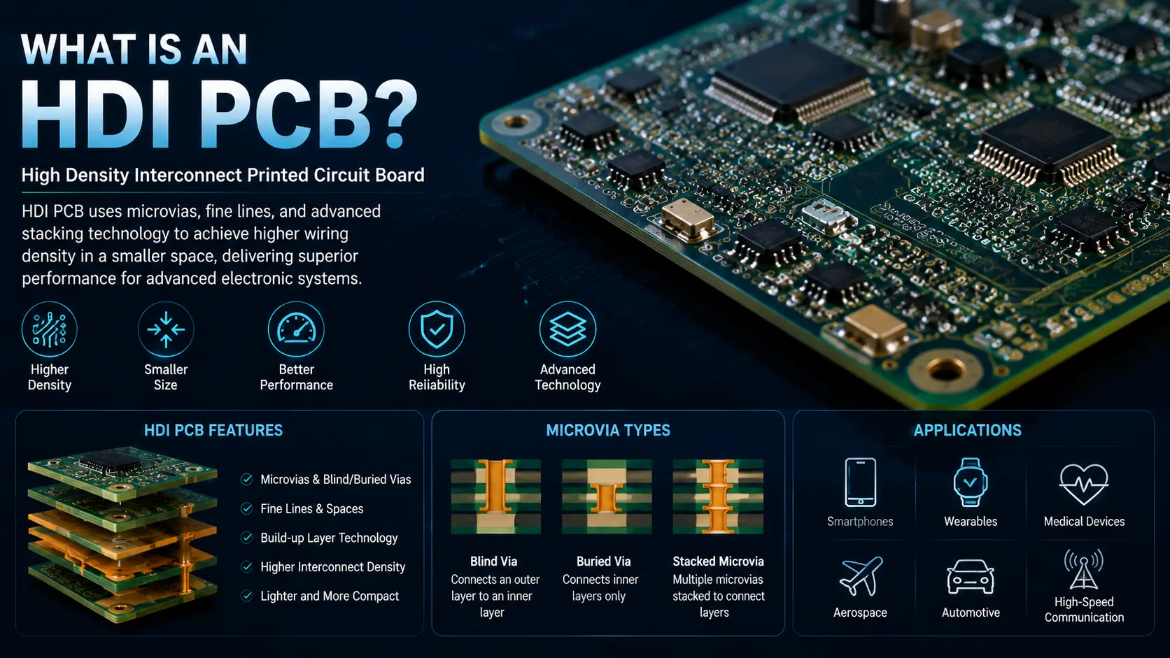
What Is an HDI PCB? Key Advantages, Structure, and Applications
HDI PCBs—or High-Density Interconnect Printed Circuit Boards—represent the pinnacle of modern circuit board miniaturization. Unlike standard PCBs, hdi boards are defined by high wiring density, microvias, blind and buried vias, fine line and fine trace widths, and advanced stackups supporting multilayer and HDI routing beyond 20 layers.
Key Advantages of HDI
- Higher circuit density: Connect more components in a smaller PCB area for smarter, thinner devices.
- Miniaturization: Enables production of smartphones, wearable devices, and implantable medical electronics impossible with traditional PCB design.
- Improved signal integrity: Ultra short traces, controlled impedance, and optimized stackups minimize noise and EMI for high-speed digital and RF circuits.
- Exceptional reliability: Advanced microvias, superior via-in-pad structures, and multilayer registration keep mission-critical boards running in harsh environments.
Popular HDI Structures
- Type I/II (1+N+1): Single build-up layer each side for simple yet dense designs.
- Type III/IV (2+N+2, any-layer HDI): Multiple build-ups using stacked vias; enables the most advanced hdi technology.
- Via-in-pad and microvia-in-pad: Allows fine pitch BGA escape, reducing routing bottlenecks for ASIC, FPGA, and chiplet PCBs.
Where HDI PCBs Are Widely Used
- Consumer electronics: Smartphones, laptops, audio earbuds, VR headsets.
- Automotive electronics: EV control units, ADAS, radar, vehicle communications.
- Medical devices: Imaging scanners, wearables, portable monitors.
- Aerospace/defense: Navigation, radar, secure communication modules.
- Industrial automation: Robotics, plant sensors, IIoT gateways.
Why HDI PCBs Are Central to Modern Electronics
Modern electronics wouldn’t be possible without PCB manufacturers in 2026 offering robust HDI PCB manufacturing capabilities. But why is high-density interconnect so crucial for next-generation products?
- Miniaturization and performance: In wearables and smartphones, every mm² counts. Using stacked microvias and via-in-pad, a top HDI PCB manufacturer can route power, ground, and signal lines in a fraction of the space, directly improving electrical performance and freeing area for batteries or antennas.
- Reliability for regulated markets: From automotive to medical, reliability can mean life or death. Premium PCB suppliers use microsection analysis, electrical testing, and thermal cycling to guarantee no latent defects, as required by ISO 9001, IATF 16949, and ISO 13485.
- Impedance and RF applications: High speed and RF PCBs require tight control of impedance. Advanced hdi PCB manufacturers achieve this with multilayer stackups and fine line geometries.
- Flexibility in design: Engineers working on multilayer and HDI designs rely on suppliers who adapt routing, stackups, and material to unique design needs—cutting NPI risk.
Key HDI PCB Capabilities & Manufacturing Solutions
What sets the best HDI PCB manufacturer apart from competitors? Here are the most essential HDI PCB fabrication companies’ capabilities:
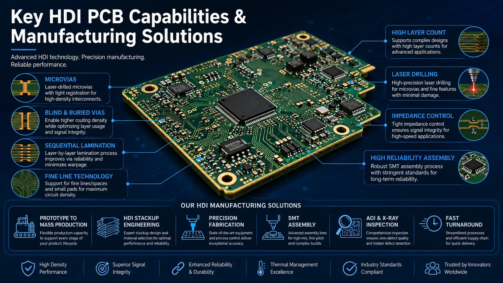
1. Microvias, Blind & Buried Vias
- Microvias (down to 50 μm) and copper-filled buried vias allow unmatched 3D routing and high current density.
- Stacked and staggered microvias offer connections across 20+ multilayer HDI stackups.
- Fact: Ibiden is known for reliability and innovation in automotive PCB stacking and microvia process control.
2. Advanced Fabrication
- Multilayer PCB manufacturing (8–56 layers) with precise registration.
- Laser drilled via-in-pad, fine line patterns, any-layer HDI, and high aspect ratio boards.
- Controlled impedance and RF stackups (critical for 5G and AI server PCB).
3. Material Science
- Support for FR4, Rogers, Isola, Megtron, and high Tg materials for diverse environments.
- Use of laminates with low loss for high-speed PCB routing and reliable signal integrity.
4. Process Control & Testing
- 100% Automated Optical Inspection (AOI) and X-ray validation for every batch.
- Full netlist electrical testing; microsection and impedance testing on request.
- Data-driven yield improvement, often using statistical process control (SPC) and continuous improvement models.
Quality Standards, Certification, and Process Control
Key Certifications for 2026
Every reputable HDI PCB supplier tracks certifications and process tolerance compliance for each circuit board produced:
- ISO 9001: Core for all manufacturers; confirms robust process control.
- IATF 16949: Automotive-grade reliability; required for advanced hdi automotive PCB solutions.
- ISO 13485: For medical devices.
- AS9100D: Aerospace and defense.
- UL & IPC Class 2/3: Product and manufacturing safety.
Some of the best PCB manufacturers provide custom dashboards for live traceability and batch-level certification. Ask your supplier about transparency and verification procedures.
Quality Assurance & Electrical Test Steps
- AOI for trace, space, and alignment issues on every HDI design.
- X-ray for buried vias/laser microvias.
- Microsection analysis on production lots.
- Electrical test (flying probe or fixture) to catch open circuits and shorts.
Top 15 HDI PCB Manufacturers Worldwide (2026)
Below are the top HDI PCB manufacturers in the world—chosen for their high-density interconnect technology, reliability, advanced circuit board fabrication, and global influence on multilayer and HDI PCB production.
1. Zhen Ding Technology (Taiwan)
- World’s largest PCB manufacturer specializing in HDI PCBs, fine line routing, high-volume HDI, and flex circuit production.
- Renowned for quality, process control, and deep certification portfolio (ISO 9001, IATF 16949).
- Essential for smartphones, consumer electronics, and high-performance automotive electronics.
2. Unimicron Technology (Taiwan)
- Leading manufacturer with advanced hdi PCB capabilities, specializing in multilayer HDI, BGA fan-out, and IC substrate PCB fabrication.
- Key supplier to the world’s largest server, mobile, and networking brands.
- Regarded for reliability in microvias, signal integrity, and robust PCB manufacturing capabilities.
3. LHDTECH (Shenzhen, China)

- Shenzhen prototype and volume HDI PCB supplier known for quick-turn, ISO 9001 and ISO 13485 certification.
- Supports prototype builds for medical devices, RF, and high-voltage industrial circuits with strong documentation and manufacturing solutions.
- Expert in advanced HDI, controlled impedance, and complex stackup PCB assembly.
4. TTM Technologies (USA/China)
- Globally recognized for complex, high-reliability, automotive and aerospace circuit board manufacturing.
- Delivers high-density solutions for regulated automotive and defense markets with AS9100D, IATF 16949, and ISO 9001.
- Robust process control for impedance, AOI/X-ray, reliability validation, and advanced test.
5. Nippon Mektron (Japan)
- Renowned for flexible HDI PCB manufacturing; global supplier of automotive electronics, smartphones, and wearables.
- Pioneers in multilayer/high-density circuits and embedded microvias meeting strict reliability standards.
6. Compeq Manufacturing (Taiwan)
- Specializes in server, automotive, and AI data center multilayer HDI with cutting-edge circuit design, high-density interconnect, and advanced hdi PCB manufacturers process.
- Consistently ranked among pcb manufacturers in the world by both market size and technological innovation.
7. AT&S (Austria)
- European high-reliability manufacturer: medical, automotive, aerospace, and industrial automation.
- ISO 13485, automotive, and defense certifications; masters any-layer HDI and advanced laminate innovation.
8. Ibiden (Japan)
- A true leading hdi pcb manufacturer focused on automotive, RF, and high-performance multilayer/HDI PCB technology.
- Advanced microvias, high-speed circuit routing, and exceptional electrical performance for demanding applications.
9. Shennan Circuits (Shenzhen, China)
- Prominent among HDI PCB manufacturers in China for telecom, 5G, high frequency, and automotive electronics PCB manufacturing.
- Known for controlled impedance, mass production, and test rigor.
10. Würth Elektronik (Germany)
- Premium European manufacturer, specializing in rigid-flex, automotive, industrial IoT, and sensor circuit boards.
- Noted for technical documentation, traceability, and DFM feedback on HDI circuit board designs.
11. NCAB Group (Sweden)
- European sourcing and QA partner, with audited fabrication partners in China.
- Ideal for regulated medical and industrial buyers seeking audit-ready, high-reliability HDI PCBs.
12. Sanmina Corporation (USA)
- North American manufacturer offering both PCB fabrication and full-system PCB assembly; strong in healthcare, aerospace, and mission-critical circuit board supply chains.
13. Meiko Electronics (Japan)
- Major automotive and consumer electronics PCB manufacturer, balancing fine trace, microvia, and high-volume HDI PCB production.
14. Samsung Electro-Mechanics (Korea)
- Semiconductor packaging leader with cutting-edge interconnect and high-layer-count HDI PCB manufacturing for mobile, AI hardware, and advanced IC substrates.
15. PCBark (Shenzhen, China)

- Rapid-turn, low MOQ pcb supplier for engineering teams, startups, and SMEs; offers instant quote, DFM feedback, and prototype delivery on FR4 and HDI designs.
Selecting the Right Manufacturer: Key Steps & Pitfalls
Step-by-step checklist:
- Start with certifications. Always confirm ISO 9001, IATF 16949, ISO 13485, and any special automotive, medical, or aerospace requirements. Good manufacturers are never shy about certificates.
- Assess circuit, layer count, and advanced HDI capabilities. Not all suppliers handle microvias, buried vias, fine trace, and via-in-pad consistently above 20 layers. Ask for sample stackups from recent projects.
- Request DFM feedback prior to prototype. World-class HDI PCB manufacturers in China and abroad offer DFM prior to PCB fabrication or assembly—saving days or weeks and boosting first-pass yield.
- Check quality and process control. Ask for sample microsection analysis, electrical test data, photos of their AOI station, and process flow diagrams—especially for new hdi pcbs.
- Trial run a prototype. Before placing volume orders, run a small lot prototype. Review yield, test results, communication, and shipping/ESD packaging.
Pitfalls to Avoid:
- Selecting by price only (risks poor reliability, lack of documentation or certification, and later recalls),
- Neglecting traceability on regulated products,
- Skipping electrical or X-ray test reports for microvias and buried vias,
- Failing to specify impedance, assembly/DFM, or reliability requirements on your RFQ.
Onshore vs Offshore Suppliers: Pros and Cons
- Onshore PCB Manufacturers (USA/EU):
- Pros:
- High certification standards (ISO 9001, ISO 13485, IATF 16949, AS9100D).
- Enhanced process control, reliable documentation, and detailed traceability—crucial for high-density interconnect and medical circuit board projects.
- Easier compliance with U.S./EU-specific reliability requirements and legal regulations.
- Fast engineering communication, strong after-sales support, and easier factory auditing.
- Lower risk for confidential designs and intellectual property (IP) protection.
- Best for critical automotive electronics, aerospace, and life-saving medical devices.
- Cons:
- Typically higher HDI PCB manufacturing and assembly costs.
- Sometimes limited in high-volume HDI production capacity and rapid scaling.
- Fewer choices for exotic or custom high-density materials compared to Asia.
- Pros:
- Offshore PCB Manufacturers (China/Taiwan/Southeast Asia):
- Pros:
- Competitive pricing, especially from high-volume Chinese manufacturers and extensive Shenzhen-based HDI PCB suppliers.
- World’s largest PCB fabrication and assembly capacity—mass production for consumer electronics, multilayer, and advanced circuit boards.
- Rapid advances in HDI technology: microvias, buried vias, and fine line innovation on par with global best practices.
- Broad material availability, quick-turn HDI PCB prototype options, and increasingly robust process control and certification portfolios.
- Shenzhen and other Chinese clusters can ship prototype and volume builds worldwide—often with online DFM and quoting portals for fast project launches.
- Cons:
- Must carefully vet credentials, documentation, and manufacturing standards; not all factories maintain true ISO 9001/certification or IPC Class 3 processes.
- Additional diligence for quality assurance, electrical test authenticity, and traceability.
- Potential geopolitics, tariffs, and logistics delays affecting supply chain continuity in 2026.
- Pros:
Tip for 2026: Many global brands use a hybrid approach: DFM and prototyping with onshore suppliers, transitioning to mature offshore manufacturing partners for high volume HDI and mass-market consumer electronics.
HDI Success Stories: Automotive, Medical, and Consumer Electronics
Automotive Electronics Reliability
A leading EV manufacturer selected Ibiden for a safety-critical radar project—demanding ISO 9001 and IATF 16949 certification, microvias with controlled impedance, and advanced hdi PCB capabilities. By auditing process control, requesting electrical test and microsection reports for every batch, and running small-lot prototypes, they achieved best-in-class reliability and zero field failures in the first 18 months.
Medical Devices: From Prototype to FDA Approval
A wearable ECG developer in North America needed multilayer and HDI, fine line, and advanced circuit boards for patient monitoring. After failures with low-tier suppliers, they switched to PCBSync (Shenzhen), requesting ISO 13485 certification, microvia test data, and complete batch traceability for pilot runs. The right manufacturer’s documentation accelerated FDA approval and scaled to mass PCB production with zero returns.
Consumer Electronics Miniaturization
A global smartphone OEM partnered with Zhen Ding Technology for its flagship 2026 device. The supplier’s high-volume HDI, microvia-in-pad design, and superior yield for fine trace routing allowed more processing power and battery in a slimmer, lighter form—cementing their leadership in the world’s largest consumer electronics markets.
Key Trends: Miniaturization, RF, and Advanced HDI Solutions in 2026
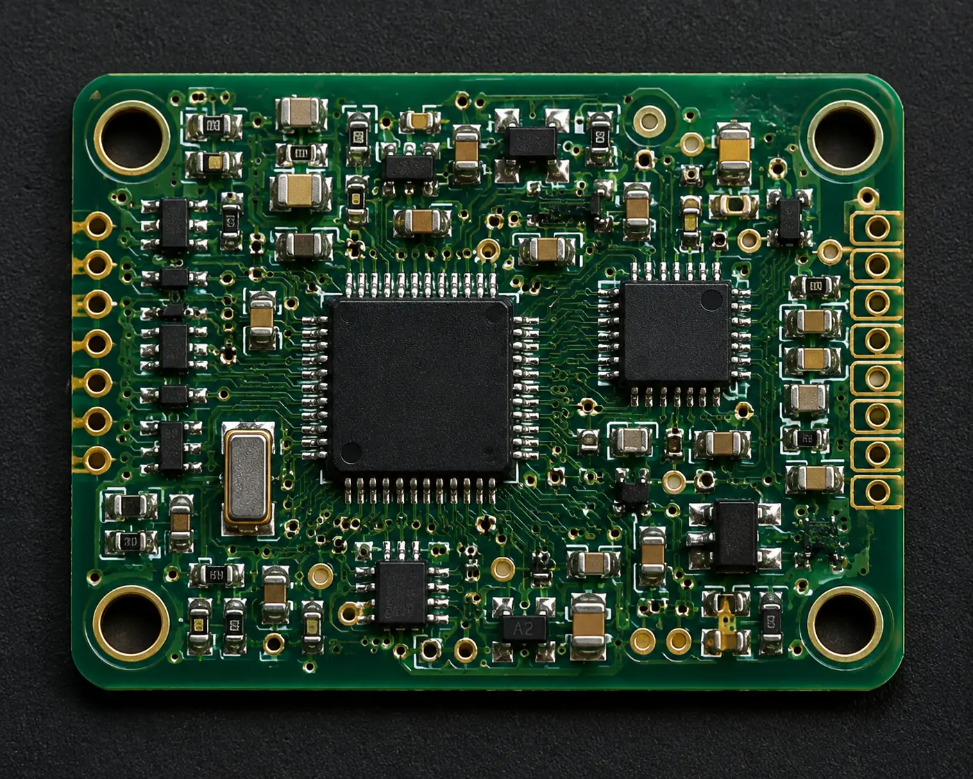
1. Miniaturization and Any-Layer HDI PCB Technology
As devices shrink, circuit density and any-layer HDI routing become standard—not a luxury. Expect more rigid-flex PCBs, microvia-in-pad, and 10/10 μm fine line builds in wearables, IoT, and medical devices.
2. Explosion of Multilayer and HDI in Automotive Electronics
2026 will see over 50% of advanced vehicle control units requiring high-density interconnect, impedance control, and buried vias for radar, infotainment, and networking. Leading HDI PCB manufacturers focus on thermal/vibration reliability, sustaining performance for over 10 years on the road.
3. High-Performance RF and Signal Integrity
Demand for high-speed, impedance-controlled, and low-loss HDI stackups is surging for 5G/6G infrastructure, AI servers, and automated factory controls. Look for suppliers with proven RF circuit board experience and robust electrical performance certification.
4. DFM Automation and Real-Time Process Control
In 2026, suppliers integrate online DFM portals, digital traceability, and inline AOI/X-ray. Advanced process control helps spot microvia voids, fine trace defects, and stackup issues—reducing scrap and boosting first-pass yield.
5. Eco-Friendly Materials and Certification
With sustainability targets tightening, top hdi pcb manufacturers are pursuing ISO 14001 certification and closed-loop process control—from laminate sourcing to PCB assembly and final shipping.
Frequently Asked Questions About HDI Designs and Manufacturing
Q1: What makes an HDI PCB manufacturer reliable for mission-critical applications?
A: Multiple industry certifications (ISO 9001, IATF 16949, ISO 13485), proven microvia and impedance testing track record, transparent process control, and batch-level traceability.
Q2: How should I evaluate PCB manufacturers in 2026 for new HDI designs?
A: Begin with certification audit, review electrical test and DFM reports, prototype trial runs, and sample stackup validation. Confirm supplier’s experience with your required microvias, fine line, and high-density requirements.
Q3: What advanced circuit board materials are best for high-frequency RF or automotive?
A: Rogers, Megtron, Isola, and high-Tg/low-loss laminates—supported by all Tier-1 manufacturers worldwide.
Q4: Can I use Chinese manufacturers for safety-regulated or medical circuit designs?
A: Yes, provided they hold genuine ISO 9001, IATF 16949, and ISO 13485 certificates, and can provide test/certification/traceability documentation for every prototype and production batch.
Q5: What’s the typical lead time for hdi PCB fabrication and assembly?
A: For quick-turn prototypes: 1–5 days (NextPCB, PCBSync, Würth Elektronik). High-volume HDI: 15–30 days at global leaders (Zhen Ding, Unimicron, TTM Technologies, Ibiden). Add time for certifications and special process testing.
Conclusion: Why the Right HDI PCB Supplier Makes All the Difference
In 2026 and beyond, choosing the right manufacturer is not a box-ticking exercise—it’s your guarantee of reliability, compliance, and innovation. The world’s largest brands don’t just buy HDI PCBs; they partner with PCB manufacturers in the world who demonstrate real-world expertise in advanced circuit boards, multilayer and HDI stackups, proven certification, and transparent process control.
Action Steps:
- Create a shortlist using this guide’s comparison table and manufacturer profiles.
- Prioritize DFM feedback, electrical test, and full transparency from RFQ through PCB assembly.
- Require sample documentation, process control evidence, and insist on certification authenticity—ISO 9001, IATF 16949, ISO 13485, AS9100D for your sector.
- Start with a prototype. Scale up only after first-pass success and validation—with clear measures for reliability, electrical test, and design-for-manufacturability.
- Stay updated—today’s leading hdi pcb manufacturer could be tomorrow’s innovation partner as miniaturization, RF, and high-density circuits keep advancing.